As stated by Moore's Law, the density and performance of integrated circuits have grown rapidly over the decades. As we all know, this trend of rapid growth will one day end, people just do not know the extent to which the density and performance of integrated circuits can reach when this moment comes. With the development of technology, the density of integrated circuits is increasing, and the width of gate oxide is decreasing. The multiple effects commonly found in very large scale integrated circuits become more important and difficult to control. The antenna effect is one of them. In the past two decades, semiconductor technology has grown rapidly, resulting in products with smaller specifications, higher package density, higher speed circuits, and lower power consumption. This article will discuss antenna effects and solutions to reduce antenna effects.
Antenna effect
Antenna effect or plasma-induced gate oxide damage refers to an effect that can potentially affect product yield and reliability during MOS integrated circuit production.
Currently, lithographic processes use integrated plasma etching (or "dry etching") to fabricate integrated circuits. Plasma is an ionized/active gas used for etching. It provides super mode control (sharp edge/less undercut) and a variety of chemical reactions that are not possible with conventional etching. But everything has two sides, it also brings some side effects, one of which is charging damage.
Plasma charging damage refers to the unintended high field stress of the gate oxide produced in the MOSFET during plasma processing. During plasma etching, a large amount of charge accumulates on the polysilicon and metal surfaces. Through capacitive coupling, a large electric field is formed in the gate oxide, resulting in stresses that can damage the oxide layer and change the device threshold voltage (VT). As shown in the figure below, the accumulated static charge is transferred to the gate and neutralized by the current tunnel through the gate oxide.
Figure 1: Antenna effects during plasma etching.
It is obvious that the area of ​​the conductor exposed to the plasma is very important, which determines the static charge accumulation rate and the tunneling current. This is the so-called "antenna effect." The area ratio of the conductor under the gate to the oxide layer is the antenna ratio. In general, the antenna ratio can be thought of as a current multiplier that amplifies the density of the gate oxide tunneling current. For a given antenna ratio, the higher the equal particle density, the greater the tunneling current. Higher tunneling current means higher damage.
3 plasma manufacturing processes
Conductor layer mode etching process - The cumulative charge is proportional to the circumference.
Ashing process - The amount of accumulated charge is proportional to the area.
Contact Etching Process - The amount of accumulated charge is proportional to the area of ​​the pass region.
The conventional definition of the antenna ratio (AR) refers to the ratio of the area of ​​the "antenna" conductor to the area of ​​the gate oxide layer to which it is connected. Conventional theory holds that the degree of reduction in antenna effect is proportional to the antenna ratio (the charging effect of each metal layer is the same). However, it has been found that the antenna ratio does not depend on the antenna effect, and layout issues need to be considered.
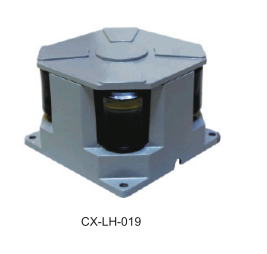
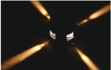
LED point light source is a new kind of energy conservation and environmental protection decorative light, using LED cold light source, the built-in microcomputer chip, can be arbitrary programming control, multiple synchronous change, monochromatic changes can also be realized synchronous colorful gradient, jump, scanning, running water light color change effect and multiple LED point light source form a lattice screen.All kinds of pictures, text and animation effects can be changed. It is a supplement of linear light source and flood lighting, which can meet the design requirements of the point line surface.


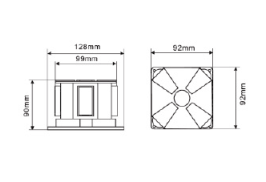
Product size

Led Point Lamp,Blue Point Led Lamp,Led Point Ovale,Led Blue Point
Jiangsu chengxu Electric Group Co., Ltd , http://www.chengxulighting.com
