
With the maturity of sub-micron, deep sub-micron technology and system-on-chip (SOC) technology, power consumption has become the primary consideration in analog circuit design, and low-voltage low-power integrated circuit design has gradually become mainstream. Since the substrate of the MOS transistor is either connected to the source or connected to VDD or VSS, it is often used as a three-terminal device.
Since the threshold voltage of CMOS technology is not far lower than the existing standards in the future, the use of substrate driving technology for analog circuit design becomes a better solution. The principle of the substrate driving technique is to add a sufficiently large fixed voltage between the gate and the source to form an inversion layer, and an input signal is applied between the substrate and the source, so that the threshold voltage can be reduced or Avoided from the signal path. The principle of a substrate-driven MOS transistor is similar to a junction field effect transistor, that is, a depletion device, which can operate under negative, zero, or even slightly positive bias conditions. Since the substrate voltage affects the thickness of the depletion layer connected to the inversion layer (ie, the conduction channel), the drain current can be modulated by changing the substrate voltage by the bulk effect of the MOS transistor.
Some basic analog circuit standard modules are built by using the substrate driving technology, and the use of the substrate driving technology in the analog circuit design is illustrated by an example.
1 simple and enhanced substrate drive current mirror
A simple substrate-driven current mirror structure, the low-voltage current mirror proposed in this paper, is shown in Figure 1(b). This current mirror replaces the gate-drain connection in a conventional simple current mirror structure with a substrate-drain connection. . Of course, M3 and M4 are connected through the substrate instead of the gate, and the gates of the N-type MOS transistors M3 and M4 should be applied with a suitable forward bias voltage.
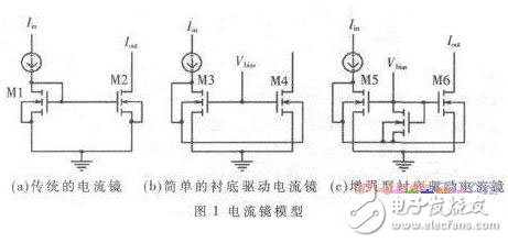
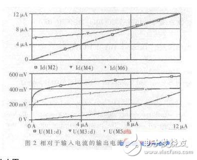
A drawback of this simple substrate-driven current mirror is that the input-output current is non-linear because the output transistor M4 operates in a saturated state in the gate drive current mirror. To solve this problem, an alternative configuration is used, as shown in Figure 1(c). The transistor M7 is used as a diode connected between the gates of the two transistors M5 and M6 and the substrate. M7 is used as a simple voltage source. When input current Iin is zero, transistor M6 operates in saturation and M5 does not. Once the input current begins to increase, the transistor M5 in the enhanced substrate drive current mirror enters saturation earlier than M3 in the simple substrate drive current mirror, thus having better linearity. Since this connection can drive both the gate and the substrate, the bias current Ibias flowing through M7 is counted in the input Iin. To avoid additional offset between the input current and the output current, the bias current Ibias must be far Less than the input current Iin. Figure 2 is a simulation result of the current mirror model in Figure 1, which shows that the input-output transmission characteristics of the substrate-driven enhanced current mirror have better linearity than the simple substrate-driven current mirror, and its linearity Almost the same as the gate drive current mirror. It can also be seen from Figure 2 that the input voltage of a simple substrate-driven current mirror and an enhanced current mirror is much lower than that of a conventional gate-driven current mirror.
2 substrate driven transconductance operational amplifier
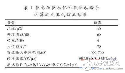
The structure of the transconductance operational amplifier based on the substrate driving technology is as shown in FIG. 3, and is composed of two stages. The first electrode is composed of a substrate driving differential stage. The differential stage is input with PMOS devices M1 and M2, and the current mirror M3. M4 acts as the active load; the second pole is a simple CMOS to phase stage that uses M6 as the drive tube M7 as the active load. The output terminal and the input terminal of the differential stage of the compensation capacitor CC and the resistor Rc are connected together, and the compensation capacitor is actually used as the Miller capacitor in the second stage.
By providing a sufficient gate-to-source voltage value to turn on the FET, the substrate-driven MOS transistor operates on the principle of a depletion mode device, and the current flowing through the transistor is modulated by an input voltage applied to the substrate terminal to complete the substrate driving. The transconductance operational amplifier design of the input transistor is shown in Figure 3. The simulation results are shown in Table 1.
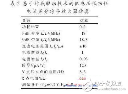
3 substrate drive current differential transconductance amplifier
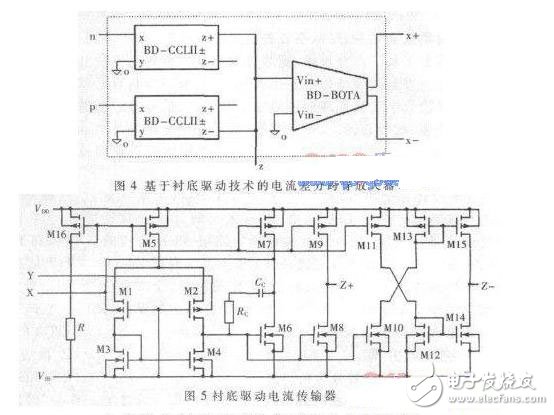
The current differential transconductance amplifier is a new active device based on a substrate driven current differential transconductance amplifier. As shown in Figure 4, it is suitable for designing large scale integrated circuit modules. This is achieved by two substrate drive current drivers as shown in Figure 5 and a substrate driven transconductance operational amplifier (dual output DO-transconductance operational amplifier) ​​as shown in Figure 3. The current transmitter is connected as a current differential unit, the current flows into the Z+ terminal of the upper current transmitter, and the current Ip flows into the Z-side of the lower current transmitter but opposite to the current of the Z+ terminal. This explains that the current flowing into the Z terminal of the current differential transconductance amplifier is provided by the differential currents Ip and In. The circuit and its simulation results are shown in Figure 4 and Table 2.
4 Conclusion
Through simulation analysis, the advantages of the substrate driving transistor are: the power consumption of the circuit is relatively low; the design is simple and acceptable circuit characteristics; the depletion characteristic required by the threshold voltage can be avoided; the traditional front end gate can be used to modulate the substrate Drive MOS transistors. The disadvantages of the substrate drive transistor are: (1) its transconductance is much smaller than that of a conventional gate drive MOS transistor, which may result in a low gain bandwidth product of the transconductance operational amplifier; (2) its electrode is process dependent, a CMOS In the P(N) well of the process, only the substrate driving MOS transistor of the N(P) channel is effective, which may limit its application.
The main control unit of the equipment is PLC and the HMI (Human Machine Interface) is 7" LCD colorful touch screen. The equipment has varieties of operating modes, and can automatically record and save working status.
The complete set of equipment is easy to operate, reliable in working, complete in protection and high in automation.
Fast Charging,Intelligent Fast Battery Charger,Agv Automatic Battery Charger,Agv Fast Charger
Xinxiang Taihang Jiaxin Electric Tech Co., Ltd , https://www.chargers.be