
Many low-power wearable devices such as smart watches, fitness wristbands and headsets are on the market (Figure 1). It is expected that in the next few years, the camp of this new electronic product series will grow rapidly. These devices are usually small and slim, with different shapes and industrial designs. The battery's capacity range may be 100mAh~300mAh, which determines the required charging rate.
This type of device is traditionally charged using a plug-in jack or a micro-USB connector. But even these smaller connectors are too big for some new ultra-thin wearable applications. In addition, connector contamination has become a more serious problem due to the outdoor wearable environment.
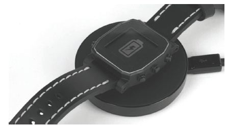
Figure 1: A smart watch with wireless charging.
Wireless charging solutions can solve these problems and provide designers with more opportunities. Existing semiconductor devices for the WPC (Wireless Charging Alliance) Qi standard can be easily adapted to such lower power applications. This technique uses two planar coils to transmit power through a sealed enclosure. For low-power wearables, the small, slim, low-power receiver coil can be easily embedded in the back of the sealed enclosure or wristband area. Qi-compatible devices are a proven solution that reduces development time and are supported by existing WPC infrastructure.
Qi compatible wireless power system
A typical wireless power system (Figure 2) has a receiver (Rx) in the portable device that provides energy to charge the battery. The transmitter (Tx) is located in a fixed base and is connected to a wall-mounted power supply. The input electrical energy is converted to alternating current, and then magnetic coupling occurs through the coil when the transmitter coil is in close proximity to the receiver coil. The receiver's output is typically 5V at currents up to 1A, which provides input power to the battery charger IC in portable devices.
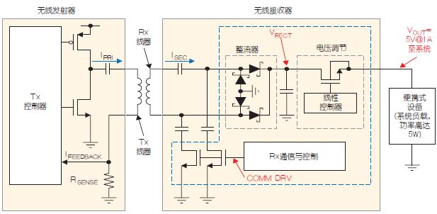
Figure 2: Block diagram of a Qi-compatible wireless power system.
The transmitter operation in the system is controlled by the receiver chip using feedback in the form of a digital communication packet that is transmitted back through the same magnetic coupling path. The Qi-compatible receiver uses load modulation to send information across the two coils in packet form to communicate with the transmitter. The transmitter coil voltage and current are modulated at a rate of 2 kHz, decoded by the transmitter and used for control. The receiver can send multiple types of data packets to the transmitter for control and information transfer. In addition, the failure of communication will terminate any power transfer.
The Qi standard "Identification and Configuration" command packet is very useful to ensure that power is only transmitted to the correct device, thus avoiding potentially dangerous situations. The "Charge Complete" and "End Power Transfer" packets are also useful commands to stop power transfer when the battery is fully charged or when other conditions require termination of power transfer (Reference 1). These features ensure safe power transfer between the transmitter and receiver using existing well-known standards.
Low power wireless system
By carefully adjusting the coil size and external component values ​​to match smaller size applications, existing Qi-compatible receivers and transmitters can be optimized for low-power wireless systems. Both the transmitter and receiver coils can be downsized to accommodate smaller shapes. The components of the power section (especially for the transmitter) reduce the power specification.
A typical WPC-1.1 Qi compatible system can support output loads up to 5W (typically 5V@1A). On the other hand, low-power systems for wearable device applications may have an output power range of 5V@100mA~250mA.
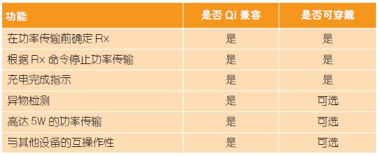
The use of most Qi compatible features does not affect size or performance. The Foreign Object Detection (FOD) feature is an optional feature that prevents stray metal objects from being transferred to the charging area. In a low power system with FOD functionality, the total output power is reduced by more than 50%. As the charging area shrinks, objects enter the area and are heated to the point where the likelihood of problems is greatly reduced. The key to FOD functionality may depend primarily on the mechanical design of the wearable device charging pad or charging dock. Table 1 summarizes some of the main features available when using the WPC-1.1 Qi standard, which are optional when customizing wearable applications.
Table 1: Comparison of Qi compatible standards with wearable solutions.
Low power system coil
The size of the coil can be reduced to a point, but still requires transmission of power and communication with the transmitter. A typical coil structure is a circular planar coil made of copper wire on a shield. An alternative configuration is a PCB or flexible circuit coil. Typically, these alternatives may have higher direct current (DC) resistance (lower efficiency), but are very thin, which is ideal for small, low-power applications. The shield prevents AC electromagnetic fields from entering the electronics and battery, which also improves the performance of the coil.
Assuming that the Rx coil and the Tx coil are aligned on the xy plane, there are two key factors that determine the coupling coefficient k. The first factor is the distance from the coil to the coil (z) and the second factor is the ratio of the diameters of the two coils. When the two coils are close together and the diameters match, the best coupling (highest k) result is produced (Reference 2). To ensure that the two coils are tightly aligned from the beginning on the xy plane, the mechanical design of the wearable device charging base or bracket should include a physical method that helps to properly position the device in the holder. Since the receiver coil is very small in this application, a slight misalignment between the Rx coil and the Tx coil may result in a significant reduction in the coupling coefficient and poor power transfer efficiency.
In a coupled inductor system (such as WPC/Qi), the coupling coefficient (k) between the primary coil and the secondary coil is usually 0.5 to 0.7. The typical transformer k will be much higher, for example 0.99. When the coupling coefficient is low A higher inductance value is required on the secondary (receiver) side to ensure that the output power requirement is met. Therefore, small, low-power devices that may have low coupling actually require higher secondary winding inductance than the standard 5W design (Reference 3), which may require higher inductance with more turns and larger shields. The receiver coil is required to achieve the required voltage gain.
Coil design
Design tradeoffs for receiver coil size include coil wire diameter, shield size, and thickness. The DC resistance of the coil reduces the efficiency of the receiver. The receiver coil design requires a specific number of turns to achieve the desired inductance. As mentioned earlier, the inductance required for a small coil is higher than that of a large coil due to a reduced coupling factor. In order to achieve a higher inductance value in a smaller space, the number of turns increases and the wire diameter decreases. The combined effect of finer wires and more turns will force the DC resistance to rise and reduce efficiency.
The shield provides a low impedance flux path and increases the inductance of the coil. In addition, the shield prevents AC magnetic fields from entering the metal body around the battery and receiver. Larger, thicker shields are better because thinner shields are at risk of high-throughput magnetic field saturation. Transmitter coil designs have fewer physical limitations. The coil can be larger and its inductance can be lower.
A typical coil for a standard 5W WPC application is an A11 type coil. This toroidal coil is about 50 mm in diameter with a thick ferrite shield behind it. Although this type of coil has been tested in a large number of applications with multiple types of receivers, it is best suited for higher power levels (3W to 5W). For lower power and reduced range receivers, many coil sizes can be reduced.
The typical inductance of the A11 coil is 6.3μH. This value should be maintained for best performance. The wire diameter can be reduced to allow for smaller coil sizes, but this will increase DC resistance losses. The size reduction can be further achieved by reducing the thickness of the shield layer. There are several types of shields that provide good performance.
Testing with a 30mm round transmitter coil works well (Figure 3). Achieving a smaller solution is not an idiot, but designers must be careful not to make a significant increase in DC resistance. The resonant converter architecture used in most WPC transmitters, even when the load is at a minimum, current flows in the primary coil. Taking into account the size limitations of the product, the DC resistance of the Tx coil must be reduced as much as practically possible to avoid excessive power loss.
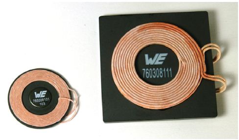
Figure 3: Standard transceiver coil and 30mm low power coil.
Low power receiver
The bq51003 is a device in the Texas Instruments wireless power receiver bq51xxx family of products designed for low power applications. A key change in this device is the optimization of several functional characteristics for lower output currents.
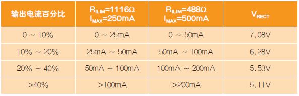
The device family features dynamic rectifier control to improve load transients (Table 2). The Qi standard has a relatively slow global feedback loop that can take up to 100ms to change the operating point. This means that the load step will lower the output voltage and cause a system reset. In order to provide sufficient voltage to cope with transient changes, the VRECT operating point needs to be set high at low loads. This feature contributes to load steps but reduces light load efficiency. To solve this problem, the dynamic efficiency adjustment function is used to adjust the light load voltage to accommodate the maximum output load. In addition, a resistor is used to set the maximum output current.
Table 2: Dynamic rectifier control for the wireless receiver (bq51003).
The heat dissipation path should also be considered due to the reduced PCB area due to power dissipation. Since typical applications require charging a small battery with a reduced charging current, the power dissipated is controllable.
As mentioned earlier, other constant voltage output receivers such as the bq51003 and bq51013B can work in conjunction with the secondary IC to regulate and manage the current to the Li-Ion battery. These batteries require precise constant current/constant voltage charge control configuration parameters that can be implemented with devices such as bq24232 (Figure 4). Simple, low-cost linear chargers are often a good choice for low-power applications. A key factor in choosing a charger device is to verify that it can control the low charge current levels required for small batteries used in wearable devices. The bq24232 can regulate constant current levels as low as 25mA when necessary and has been used in applications where small batteries are used.
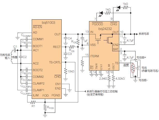
Figure 4: Wireless power receiver (with battery charger) for low power applications.
Low power transmitter
For typical applications with a power of 5W, there are many types of Qi transmitters with various features. The bq50xxx series supports receiver output power of 5W or higher. For low power applications, the bq500211 is a good starting point. It offers a standard EVM kit with a single-coil 5V input, A11 transmitter coil. However, as mentioned earlier, for lower power consumption wearable applications, such coils can be replaced with smaller components. The device can be optionally powered from a USB port or a low power 5V power adapter. The transmitter design also has a small, low cost option.
The bq500211 Qi Transmitter Controller has an input power limit option that limits the input current to the transmitter to 500mA, allowing operation via a USB port or a small power adapter. This is ideal for low power receivers that require low current. Figure 5 shows an example of a block diagram. The input current is sensed across the resistor and amplified by the current sense amplifier. The power section uses power stage MOSFETs with integrated drivers. However, separate drivers and low loss MOSFETs can be used to reduce cost. As mentioned earlier, the FOD protection function is optional when the output power is low; the circuit shown in Figure 5 does not implement the FOD function. Additionally, the design in Figure 5 does not show an optional circuit for the low power standby mode for simplicity and cost reduction.
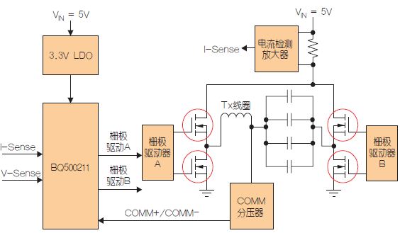
Figure 5: Low power transmitter.
in conclusion
Now, it is possible to implement wireless inductive charging in low-power wearable designs with existing custom devices. One of the key factors in designing a working solution with a power range of 500mW to 1500mW is the optimization of the magnetic components - specifically, to match the smaller size receiver coils to the corresponding smaller size transmitter coils. To maintain the best coupling coefficient. In addition, appropriate external circuit modifications were made with the bq500211 transmitter and the bq51003 low-power receiver to minimize system power loss.
references
1. Bill Johns, “An IntroducTIon to the WirelessPower ConsorTIum standard and TI's compliantsolutions,†Analog Applications Journal (1Q2011).Available:
2. E. Waf fenschmidt and Toine Staring, "Limitation of inductive power transfer for consumer applications," 13th European Conference on Power Electronics and Applications (EPE2009), Barcelona, ​​Spain, 8-10 Sept 2009, paper #0607.
3. Bill Johns, Tony Antonacci and Kalyan Siddabattula. "Designing a Qi-compliantreceiver coil for wireless power systems," Analog Applications Journal (3Q 2012). Available:
BLPS laser safety protective device is designed for personal safety used on hydraulic bender.
The dynamic test technology it used has passed the Type 4 functional safety assessment by TUV, and get the national invention patent. The product reaches the advanced technological level of similar products.
BLPS laser safety device provides protection zone near the die tip of the bender to protect fingers and arms of the operator in close to the upper mold die tip. It is the most effective solution so far to preserves the safety and productivity of the bender.
Press Brake Protection,Laser Guarding Device,Press Brake Guarding Systems,Press Brake Guarding
Jining KeLi Photoelectronic Industrial Co.,Ltd , https://www.sdkelien.com