
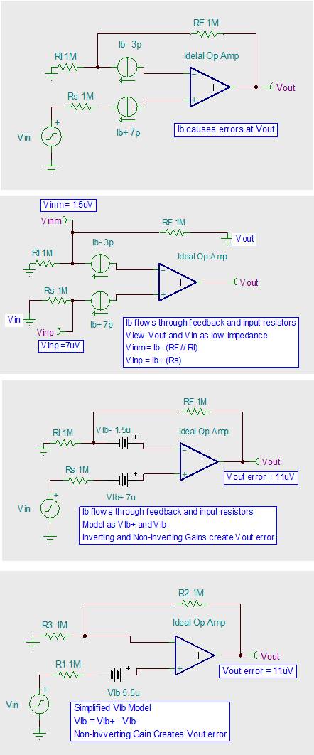
The first section describes the op amp's input bias current Ib and the input offset current Ios. It is well known that the ideal op amp has no input bias current Ib and input offset current Ios. But each actual op amp will have an input bias current Ib and an input offset current Ios. We can use the model in the figure below to illustrate their definition.

The input bias current Ib is due to the presence of leakage current (which we will call leakage current) at both input poles of the op amp. We can understand that the input terminals of the ideal op amp are connected in series with a current source, and the current values of the two current sources are generally different. That is to say, in actual operation, there will be current flowing into or out of the input of the op amp (not the same as the virtual amp of the ideal op amp). Then the input bias current defines the average of these two currents, which is well understood. The input offset current is defined as the difference between the two currents.
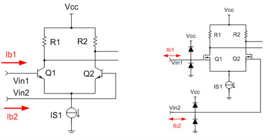
After the definition, let's take a look at the source of this current. Then we have to look at the input stage that is shipped in. The input stage of the op amp typically uses a differential input (voltage feedback op amp). The tube used is either a bipolar bipolar or a FET FET. As shown in the figure below, for bipolar, to make it work in the linear region, it is necessary to provide a bias voltage to the base, or to have a relatively large base current. It is also said that the triode is a current control device. Then the bias current is derived from the base current of the triode in the input stage. Since it is difficult to completely match the two tubes in the process, the base currents of the two tubes Q1 and Q2 always have such a difference. That is the input offset current. The two values of the oppolar input op amp are still considerable, that is to say, they are relatively large, and have to be considered when designing the circuit. For the FET input op amp, because it is a voltage-controlled current device, it can be said that its gate current is very small, usually in the fA level, but unfortunately, each of its input pins has a Protection diode for ESD. Both of these diodes have leakage currents. This leakage current is generally much larger than the gate current of the FET, which is also the source of the bias current for the FET input op amp. Of course, the two pairs of ESD protection diodes are not completely identical, so there are different leakage currents, and the difference between the leakage currents constitutes the main component of the input offset current.
The table above is the input bias current and input offset current of the bipolar LM741. This current flows to the external resistor. Even if it is K-class, it will generate an offset voltage of several tens of uV. After amplification, it is easy to Will cause the output voltage error to mV level. The following table shows the input bias current and input offset current of the CMOSFET's OPA369. These two values are much smaller. The better value of the better COMS op amp input bias current and input offset current can be less than 1pA. aims.

It is also emphasized here that the reverse leakage current of the ESD is related to its reverse voltage. Therefore, when Vin=(Vcc-Vss)/2, the voltage applied to the two ESD protection diodes is equivalent, and their reverse currents can be considered to be approximately equal. Ideally, no current flows in or out. Is the current reaches a minimum. Therefore, there is a minimum bias current. When the voltage at the input of the op amp is not equal to (Vcc-Vss)/2, it will inevitably cause the reverse voltage of one diode to be high and the other to be low. The current is not equal, and this difference current constitutes the main component of the input bias current. This scene is called the collar effect. Therefore, to minimize the FET input bias current, set the common-mode voltage to (Vcc-Vss)/2.
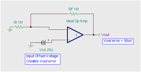
The definitions and sources are analyzed above. Let's talk about the influence of these two parameters on the circuit. The input bias current will flow through the external resistor network, which will be converted into the offset voltage of the op amp. After the operation, it will reach the output of the operation. The input error of the op amp is caused. This also explains why, in the reverse amplifier circuit, why a resistor is connected to the non-inverting input of the op amp. And this resistance should be equal to the value of the reverse input and the feedback resistor in parallel. This is to make the two input terminals bias current flow through the resistor, the voltage values are equal, so that they introduce an offset voltage of zero. To put it this way, it is too abstract, but it is easy to understand some of the following diagrams.
Another point is that for the circuit of small current detection, it is generally a transimpedance amplifying circuit, such as a photodiode detecting circuit. Generally, the optical power signal which is relatively weakly converted by the optical signal is weaker, and is often nA level rather than pA level. The intention of this circuit is to let the photocurrent flow to the feedback resistor to generate a voltage at the output of the amplifier circuit. If the op amp's input bias current is too large, just a portion of this faint photo current will flow into the op amp's input without a preset I/V linear conversion.
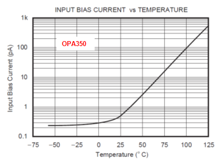
Also note that many of the op amp's input offset currents vary with temperature. As shown in the figure below, the OPAl350's input offset current rises rapidly above 25 degrees. The input bias current at 100 degrees is several hundred times that of 25 degrees. If the system is designed to operate over a wide temperature range, this factor has to be considered.
The above mentioned the input bias current and offset current of the op amp, I hope to be useful to everyone. The other parameters are detailed in the next section.
2—How to measure the input bias current Ib, offset current IosThe previous section talked about the op amp input bias current and input offset current. This section gives an input bias current measurement method. In general, there are two main test methods. One is to let the input bias current flow into a large resistor to form an offset voltage, then amplify the offset voltage and measure it, so that the input bias can be calculated backwards. The method is to let the input bias current flow into a capacitor, and integrate this current with a capacitor, so that the bias current of the op amp can be calculated by measuring the rate of change of the voltage across the capacitor.
First introduce the first method, the specific circuit is shown below, C1 is the lead compensation capacitor to prevent the circuit from oscillating, according to the actual circuit selection. The OP2 is a test-assisted op amp that requires an op amp with low bias voltage and low bias current. Test steps and principles are calculated step by step.
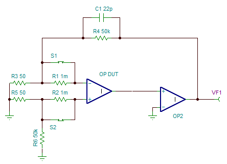
(1) First test the offset voltage of the op amp. Turn off S1 and S2 and test the output voltage of the OP2 op amp to record Vout. Then the input offset voltage is:

(2) Turn on S2, Ib+ of the op amp to be tested flows into R2, an additional offset voltage Vos1 is formed, and the output voltage of the OP2 op amp is tested to record Vout1. Then the op amp input offset voltage is:
(2) Turn off S2, turn on S1, Ib- of the op amp to be tested flows into R1, an additional offset voltage Vos2 is formed, and the output voltage of the OP2 op amp is tested to record Vout2. The op amp reverse input offset voltage is:
(4) The op amp input bias current is
Ib=[(Ib+)+(Ib-)]/2
The op amp input offset current is
Ios=(Ib+)-(Ib-)
This test method has several drawbacks. One is the use of large resistors R1 and R2, which are typically M-ohms, which introduce large voltage noise. Limited by the resistance of resistors R1 and R2, it is difficult to measure the bias current of the FET input op amp.
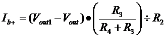
The second method of testing is to let the input bias current of the op amp flow into the capacitor. The specific test is shown below. The principle of the test is easily understood from the formula in the figure. The key to this test is to select a capacitor with a very small leakage current.
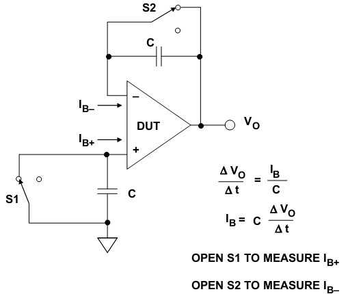
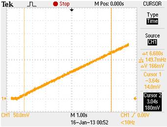
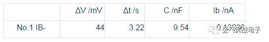
(1) Turn on S1, IB+ flows into capacitor C, and observe the change of Vo with an oscilloscope. The result is as shown below. According to the above method, IB+ can be calculated.

(2) Turn off S1 to turn on S2, IB- into capacitor C, and observe the change of Vo with an oscilloscope. As a result, as shown below, IB- can be calculated.
(3) The input bias current and offset current of the op amp can be calculated according to the definition.

This test method can measure the offset current of the fA level. Low leakage current capacitors are required for testing. Teflon capacitors, polypropylene (PP) capacitors or polystyrene capacitors with very low leakage current are recommended.
Another experience is shared. In the soldering process, the leakage current of the FET op amp is greatly increased due to impurities such as solder paste remaining on the pins. I have tested an op amp with a bias current of less than 10pA. Since there is no cleaning of the pin, the result is a large error, or error, which is up to the level of nA.
3—Input offset voltage Vos and temperature driftIn the application of the op amp, the input offset voltage Vos problem of the op amp is inevitably encountered. Especially when the DC signal is amplified, due to the presence of the input offset voltage Vos, the output of the amplifier circuit always superimposes what we do not expect. error. For a simple, old-fashioned, classic example, due to the presence of the input offset voltage, our electronic scale will have a weight display when it has not been adjusted. We don't always hope that the weight we buy is different from the actual one. It is almost nothing to buy an apple. If you buy a platinum ring, you can get a lot of money. The following describes the offset voltage of the op amp and its calculations. Finally, introduce some low input offset voltage op amps. Inadequacies, a lot of bricks.
Ideally, when the input voltages of the two inputs of the op amp are the same, the output voltage of the op amp should be 0V, but the actual situation is that even if the voltages of the two inputs are the same, the amplifier circuit will have a small voltage output. As shown below, this is caused by the input offset voltage of the op amp.
Of course, the strict definition should be that in order to make the output voltage of the op amp equal to 0, it is necessary to add a small voltage to the two inputs of the op amp. The small voltage that needs to be added is the input offset voltage Vos. Note that the output offset voltage is added to the output voltage instead of the input voltage, and the output offset voltage is divided by the gain (small difference).
The input offset voltage of the op amp is derived from the mismatch between the two tubes of the differential input stage of the op amp. As shown below. This mismatch is inevitable due to process level limitations. The mismatch of the differential input stage is a bad boy, and it will cause many other problems, which will be introduced later.

I have consulted a senior op amp design engineer. According to him, the matching degree of the two pipes is proportional to the square root of the area of the pipe within a certain range, that is, the matching degree is increased by twice. The area has to be increased by four times. When it reaches a level, even if the area is increased, the matching will not be improved. Increasing the area is to increase the cost of the IC. There is a commonly used method, which is to test after the op amp is produced, and then Trim (can be understood as tuning). This will increase the accuracy of the op amp. Of course, both testing and Trim cost. Therefore, the price of precision op amps is relatively expensive. This is only a chat, hehe.
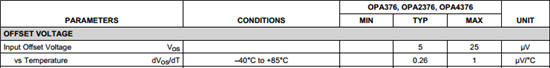
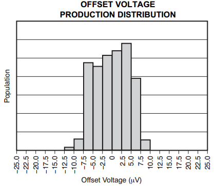
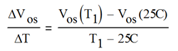
We focus on the input offset voltage because it introduces errors into the amplifier circuit. The following is an analysis of the error it brings. Before the calculation, we will recognize a parameter that makes us not too cool, the temperature drift of the offset voltage, that is, the input offset voltage mentioned above will change with the temperature. And the temperature of the application environment of our actual circuit always changes, which brings us a tough problem. The table below shows the parameters taken on the OPA376 datasheet. It has a maximum temperature drift of 1uV/°C (-40°Cto 85°C). The Vos of a large number of op amps are normally distributed, so the datasheet will generally give a histogram of the offset distribution.
When the temperature changes, the input offset voltage temperature drift is defined as:
Another important parameter that has just been forgotten is the long-term drift of the op amp input offset voltage , which is usually given like uV/1000hours or uV/moth. Some datasheets will give this parameter.
The following example calculates the maximum offset voltage of the OPA376 at 85 °C, mainly in two parts, one is the input offset voltage at 25 degrees, and the other is the offset voltage drift caused by temperature changes.
The specific steps are as follows. From the results, it seems that 1uV/°C temperature drift is the dominant error when multiplying the temperature change. Therefore, if the circuit is designed to be used over a wide temperature range, special attention should be paid to temperature drift.
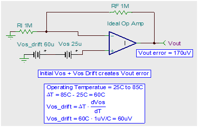
Vos (85 ° C) = 25uV + 60uV = 85uV.
If the Gain of the amplifier circuit is changed to 100, the maximum output offset voltage is 8.5mV. This is the worst case.
The test on the input offset voltage is described in "Detailed Explanation and Analysis of Op Amps Parameters - part2, How to Measure Input Bias Current Ib, Offset Current Ios". If you are interested, you can check it out. There are also simple test methods, as shown below:

Vos = Vout/1001
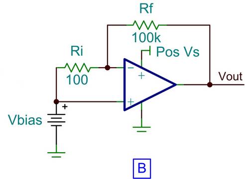
Need to be reminded that when using an easy method to test the input offset voltage of a single-supply op amp, you need to short the input and provide a low-noise, stable voltage bias. As shown below.
Below are some low temperature drift amplifiers with a maximum drift of only 0.05uV/°C. The input offset voltage Vio has a maximum value of only 5uV.
4—Rapid calculation of op amp noiseThis article is not about the noise theory of op amps. TI's senior application manager Art Kay has written a series of articles to analyze the noise of op amps. I believe most analog circuit engineers have read them. There are engineers in China who translate it into Chinese.
Today, I mainly analyze the noise composition of the op amp circuit from the top-down perspective. The main points of the calculation are the main points and the most interesting place. The most important thing is to provide you with a convenient calculation tool. It is very easy to use and let the noise The calculation becomes simple.
In the reverse amplification circuit composed of op amps, the noise mainly comes from three aspects.
(1) The input noise voltage of the op amp en (data and curve in the datasheet)
(2) The input current noise of the op amp in (data and curves can also be found in the datasheet). This needs to flow through the resistor and convert it into voltage noise.
(3) Setting the thermal noise of the resistors R1 and Rf of the amplification factor, that is, can be calculated by the classical formula. Noise = √ (4kTKRΔf). This is inevitable. In many cases it will be the main source of noise.
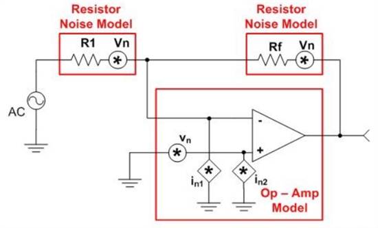
The calculation of the op amp noise is to find these three values one by one, since these noises are irrelevant. Their vector sum is the total input noise of the op amp. Then multiply the noise gain to get the output noise, the formula is as follows. It seems to be simple and it is very troublesome.

We add the calculated and input total noise to the positive input of the ideal op amp to get the noise model of the op amp. Note that it is the positive input terminal, so the gain of the noise is G=1+Rf/R1 regardless of the same-direction amplifying circuit or the inverse amplifying circuit. We can simply understand that noise is a signal that is superimposed on the input of the op amp. As shown below

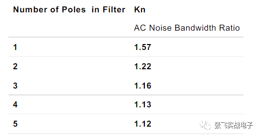
The above mentioned an important issue, the noise gain of the op amp. An important issue is also the noise bandwidth of the op amp. The op amp noise parameters given in the datasheet are generally spectral density values such as 1.1 nV √ Hz. That is to say, it is necessary to integrate it in the noise bandwidth to obtain the RMS voltage value of the noise. The noise bandwidth is different from the -3dB bandwidth of the signal. Specifically, the bandwidth of the Brickwall filter. To put it simply, the actual filter response curve is converted to the bandwidth of the rational low-pass filter when the area is guaranteed to be constant. Fortunately, we can look up the table, the -3dB bandwidth of the N-order filter and the bandwidth conversion factor of the Brickwall filter. As shown in the table below
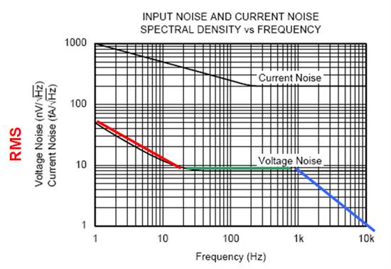
It seems to be troublesome, don't worry, and the more troublesome thing is that the op amp's input voltage noise and input current noise are frequency dependent. At very low frequencies (0.1Hz-10Hz), it is mainly 1/f noise. In the future, it is mainly white noise, as shown below.
It needs to be segmented into points.
The following figure shows the calculation of the noise voltage. As long as the value of 1/f noise at a specific frequency and the value of flat noise are input, the noise density at different frequencies can be calculated. By inputting the start and stop frequency of the frequency band, the punctuality rate of each noise in the lower frequency band can be analyzed.

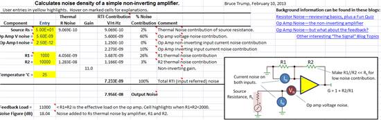
The figure below is a method to calculate the noise density of the same-direction amplifier circuit (take OPA627 as an example). You only need to input the signal source resistance, op amp voltage noise, op amp current noise, resistance value and temperature to calculate the noise of the output circuit. Density, which greatly increases the computational efficiency. The calculation results also give the punctuality rate of each noise source, which is convenient for us to optimize the noise.
This section talks about the power supply rejection ratio of the op amp. In an ideal op amp, the characteristics of the op amp do not change as the supply voltage changes. Of course, when analyzing an ideal op amp, the power supply we use will also be assumed to be an ideal power source. However, this is not the case. Actual op amps will always cause changes in the op amp parameters when the power supply voltage changes. This leads to an important parameter of the op amp, the op amp's power supply rejection ratio PSRR. The detailed definition of PSRR is given in Wikipedia. When the power supply voltage of the op amp changes, it will cause the change of the input offset voltage of the op amp (and the offset voltage). The ratio of these two changes is the op amp. PSRR. As follows
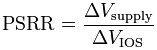
Usually expressed in dB. PSRR = 20log (⊿Vcc/⊿Vios). In some data sheets, the ratio of the offset voltage to the power supply change is also indicated. The unit is generally uV/V. As shown in the figure below, it is a representation in the datasheet of OPA365 . This is not difficult to understand. We don't have to be sad to find the ratio dB value defined by the above formula. Both of these representations allow us to clearly understand the op amp's ability to suppress supply voltage variations.

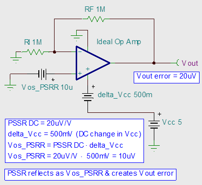
The reason why the PSSR is a finite value is also due to an incomplete matching of the op amp differential input transistors. The following focuses on its impact. The following figure is a calculation example for the OPA376 op amp. When the power supply voltage changes by 500mV, it will cause a change in the input offset voltage of 10uV. If the amplification factor is 2, the output will change to 20uV. Some circuits have a larger amplification factor, and the output offset voltage changes greatly. This is enough to cause an error in the signal delivered to the 16bits ADC. (The change in one LSB of a 16-bit ADC is 15 ppm of FSR).
The DC power supply rejection ratio is discussed in the previous section. In the actual application circuit, the power supply voltage of the op amp may be constant.
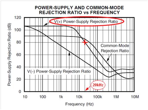
Let's analyze another key parameter, the op amp AC power supply rejection ratio AC-PSRR. This parameter is more valuable than the actual application circuit, but it is often overlooked. The DC PSRR is often given in the datasheet parameter table of the op amp. AC-PSRR is often given in the form of a chart, and we often ignore the information in the chart. However, what we ignore is often the key. The following figure shows the PSRR chart in the datasheet of the OPA376. From the chart we can see two pieces of information: (1) PSRR decreases with the increase of the AC frequency of the power supply, and (2) The AC-PSRR of the positive and negative power supplies is different.
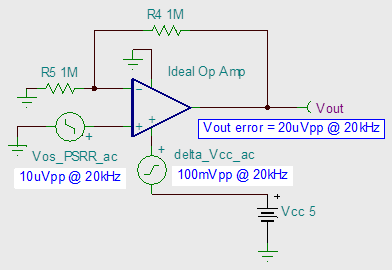
The above two points will cause unpleasant problems in the application circuit. The following figure shows a peak-to-peak value of 100mV on the power supply and a ripple of 20kHz, which will increase the output of the amplifier circuit by 20uV, 20kHz. Noise signal.
 Typically, an op amp's application circuit uses a linear power supply to power the op amp and filter the op amp's power supply. However, in some handheld devices, in order to improve efficiency and reduce power consumption, it is necessary to use a switching power supply to supply power to the operational amplifier. The frequency of the switching power supply often exceeds 100 kHz, even to the level of MHz. At this frequency point, the PSR capability of the op amp drops very quickly. If the OPA376 is at 100kHz, the PSRR is only 50dB. It is a far cry from DC-PSRR above 100dB. Another problem is that in a single-supply hand-held device, the "buck-boost" of the switched capacitor is often used to convert the positive supply to a negative supply. Seeing the AC-PSRR of the op amp on the negative power supply in the above picture will give us some cold sweat. The PSRR of the op amp is the change in the input offset voltage caused by the change in the supply voltage. Therefore, the PSRR can be measured by referring to the method of measuring the offset voltage. The PSRR can be calculated by changing the supply voltage by ⊿Vcc and then measuring ⊿Vios.
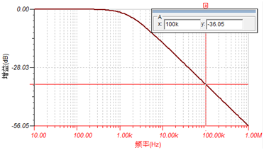
As mentioned above, when the op amp is powered by a switching power supply, the PSRR drops as the frequency increases. This causes a large ripple noise at the output. The following provides an easy way to work only with low power op amps. Add a small resistor between the DC-DC output power supply and the op amp's power supply (as shown below) if the op amp's power consumption is less than 5mA. Then this 10 ohm resistor produces a voltage drop of less than 50 mV.

Let's take a look at the effect of this circuit. The frequency response is -36dB at 100kHz, which is equivalent to a 36dB PSRR for the op amp. This power loss is worthwhile in exchange for this effect.
Another effective method is to filter the core capacitor to the power supply. The core capacitor is a three-terminal capacitor, but compared with the conventional three-terminal capacitor, since it is directly mounted on the metal panel, its grounding inductance is more Small, almost no lead inductance, in addition, its input and output are separated by a metal plate, eliminating high frequency coupling, these two characteristics determine the filter capacitance of the feedthrough capacitor close to the ideal capacitance. For the core capacitance, you can refer to the relevant information if you are interested.
7—Common mode rejection ratio CMRRThe common analog ratio of op amps is an op amp parameter that is often of interest to everyone, especially in differential amplifiers and instrumentation amplifiers. However, this section only discusses the common mode rejection ratio of the op amp and the error that the CMRR brings to the op amp. The differential amplifiers and instrumentation amplifiers are discussed later.
Before we start to discuss the common mode rejection ratio of the op amp, let's first understand the common mode input voltage of the op amp. The common mode input voltage of the op amp refers to the average of the voltages of the two input pins of the op amp. Note that the average is "This is very important, as shown below. For op amps with bipolar input stages, the op amp's common-mode input voltage typically does not reach the power rail. Some rail to rail input op amps have a common mode voltage that can reach the power rail.

Cold Shrink Tube,Cold Shrinkable tubing,Cold-shrink tube,Cold shrinkage pipe,shrink tube,Cold Shrink Cable Accessories
Mianyang Dongyao New Material Co. , https://www.mydyxc.com