
FPGA is a kind of "semi-custom" chip. One of the features is that the IO port is programmable. This feature can greatly help the programmer to interconnect with various packaged chips.
The pin functions of the MCU are fixed, and the external interface usually uses an IO port or a bus connection. Ordinary IO port is essentially a register. These registers have a corresponding address. The operation IO port is the operation register. The on-chip peripheral is relatively a function module, and its internal contains multiple registers to control different functions. But these registers also have fixed addresses. Through the way of memory mapping, the on-chip peripherals and the CPU are connected to form a system.
It is worth noting that the external interfaces of these on-chip peripherals are fixed pins. If you want to control the specific functions of these peripherals, you have already implicitly controlled these pins. For example, SCK and SDA of MUC's IIC interface are allocated at 99 and 100 feet, then all IIC interface memory chips must be connected to these two pins, as shown in Figure 1.
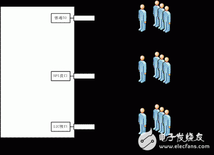
Figure 1 Please queue up
If all kinds of chips that need to be programmed need to be connected to the MCU, they must be connected with the corresponding interfaces. For chips with many complicated pins, the layout and routing of the PCB has great limitations and challenges.
FPGAs are known for their flexibility, and programmable IO is one of the key features. Programmable IO brings flexibility to the design of the PCB, which simplifies the layout of the PCB, and during the design process, the pin connections can be changed according to the direction of the trace. In addition, in the internal logic design process of the FPGA, the function module design and the pin assignment can be separated in two steps. After the internal logic function is completed, the pin is allocated according to the actual situation. Therefore, programmable IO brings certain flexibility and independence to FPGA logic design and PCB design. It acts as a “Thousand Hands Guanyin†in this link, paving the way for logic design and PCB design, as shown in Figure 2. Shown.
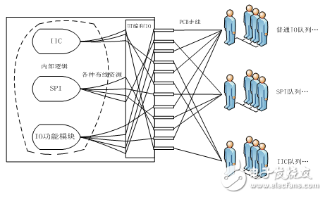
Figure 2 Schematic diagram of programmable IO
The actual FPGA is not as simple as Figure 2, just to illustrate that programmable IO can make internal logic and PCB relatively independent design. For similar interfaces, it is not necessary to change the timing logic due to PCB changes. Only the pin assignment needs to be changed, which greatly simplifies the wiring of the PCB.
Is the FPGA called "Avalokitesvara" only a large number and flexible? He has more powerful features, which are internal logic programmable.
In the original circuit design, the FPGA did not have the actual circuit, and only after the design was completed, there was a specific functional circuit. This structure contains the following features:
1. Under ideal conditions, multiple interfaces can be implemented;
2, can achieve accurate timing, compatible with more chips;
3, resources can be reused, in a certain period of time, only one interface logic is needed to save FPGA resources and configure device storage space.
In contrast, if implemented with an MCU, it has the following disadvantages:
1. If the MCU does not have a corresponding interface, it will be difficult to communicate with the memory chip containing the interface (may use IO emulation);
2, even if the interface is the same, because the function is basically fixed, in the face of some special chips, it will not work;
3. The PCB wiring with the external interface cannot be realized due to the fixing of the output port line;
There are many types of chip interfaces to be programmed, such as IIC and SPI. If the MCU has these interfaces at the same time, the port lines must be complex and have limited speed. The FPGA does not need to consider this problem. Since its internal logic can be designed by the designer, the programmer can customize the corresponding logic according to the interface needs, saving time and effort and high efficiency.
Flexibly use the FPGA "Thousand Hands Guanyin" in the design process to make the programmer function more flexible and efficient.
GFCI, or Residual Current Device (RCD) is a device that shuts off an electric power circuit when it detects that current is flowing along an unintended path, such as through water or a person.
It is used to reduce the risk of electric shock, which can cause the heart to stop or cause burns. They can also prevent some fires, like when a live wire touches a metal conduit.
Waterproof Cover UL,Wholesale Waterproof Cover UL,Color Waterproof Cover UL,Cheap Waterproof Cover UL
Hoojet Electric Appliance Co.,Ltd , https://www.hoojetgfci.com