
Currently, solid-state micro-optical devices are mainly EBCCD and EMCCD devices. With the development of CMOS technology and circuit design technology, the performance of low-light CMOS image sensors is constantly improving. By adopting special technology, the performance of low-light CMOS image sensors is close to EMCCD. The performance, unveiled the prelude to the application of CMOS image sensors in the field of low light. With the further research on low-light CMOS image sensors, in the near future, the performance of low-light CMOS image sensors will meet the requirements of night vision applications, occupying an important position in the field of micro-optical devices.
The readout circuit is an important part of the low-light CMOS image sensor. Its basic function is to convert the weak current, voltage or resistance change of the detector into an electrical signal that can be processed by the subsequent signal processing circuit. Its noise level limits the CMOS image. The application of the sensor in low light. The output signal of the pixel is very weak under low light conditions. Any excessive circuit noise and offset can annihilate the signal. Therefore, improving the SNR of the output signal of the readout circuit is one of the keys to the low-light design. The new capacitive feedback transimpedance amplifying readout circuit CTIA circuit used in this paper can provide very low detector input impedance and constant detector bias voltage, which is very low in the background range from very low to very high. The noise, the linearity and uniformity of the output signal is also very good, suitable for the reading of weak signals.
1 circuit design
To achieve accurate conversion of the detector output current to voltage, the designed circuit consists of CTIA and correlated double sampling (CDS), a reset integrator consisting of an inverting amplifier and a feedback integral capacitor. The amount of gain is determined by the integral capacitance. Figure 1 shows the typical CTIA circuit structure.
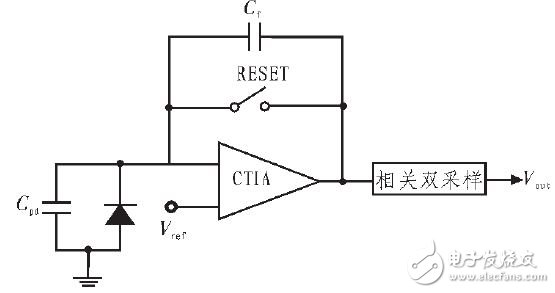
Figure 1 Typical CTIA structure
When the Reset signal is high, the MOS switch is turned on. It can be seen from the virtual short characteristic of the operational amplifier that the voltage at the input terminal is equal to Vref. At this time, the voltage across the integrating capacitor is equal, and both are Vref. When the Reset signal goes low, the MOS switch is turned off. Since the voltage at the input is controlled by Vref, the induced charge is generated on the right plate of the integrating capacitor Cf and slowly accumulates. The voltage of the right plate gradually increases, and the integration process begins. . The final voltage is read out by the correlated double sampling circuit.
2 key unit circuit design
2.1 High Gain Low Noise CTIA Circuit
In order to increase the gain of the readout circuit, the circuit can read the current of the PA stage in a relatively short integration time, and the integral capacitance in the circuit is very small. At the same time, in order to improve the signal-to-noise ratio, the circuit noise is also reduced while reducing the integral capacitance. In the new circuit structure, the T-type network capacitor plus the nmos switch is used, and the circuit structure is shown in Figure 2.
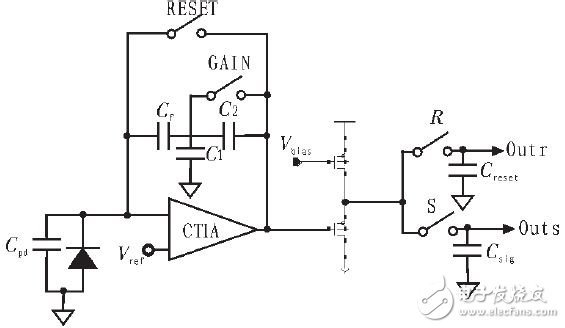
Figure 2 High-gain, low-noise CTIA circuit
Due to the action of C1 and C2, the effective value of Cf in the CTIA feedback loop is reduced. The effective value is Cfb=( C2Cf)/(Cf +C1+C2), so that Cf can take a relatively large value and avoid Use small capacitors because small capacitors are difficult to implement in the process and have large errors. In this circuit, Cf=20 fF, C2=18 fF, C1=150 fF, then Cfb=2 fF.
Figure 3 shows the timing of the operation of this circuit.
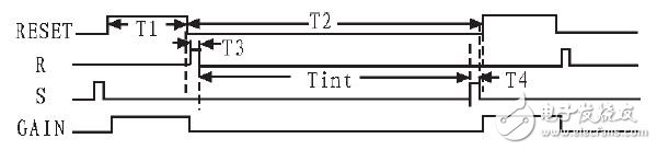
Figure 3 High-gain low-noise CTIA circuit operation timing
This circuit can operate in either high gain mode or low gain mode. In high gain mode, when reset is high, gaIn is turned on, then the effective capacitance is Cf, when reset is low, gaIn is turned off, and the integral capacitor at this time is a T-type network composed of Cf, C1, and C2. Capacitor, this ensures a large capacitance of the circuit at reset, which can effectively reduce noise, and small capacitance during integration can greatly improve the gain. When gaIn is always high, the circuit operates in low gain mode.
2.2 Related double sampling
The related double sampling circuit consists of two sets of capacitors and switches. The circuit works as follows. First, the integration is started, R is turned on, and the correlated double sampling circuit first reads out the reset signal of the pixel, and stores the Vreset voltage into the capacitor Creset. After the integration is completed, the switch S is turned on, and the voltage Vread is stored in the capacitor Csig. Finally, the voltage values ​​stored above the two capacitors are subtracted to obtain the final pixel output voltage value:
Vout=Vouts -Voutr
This structure can well eliminate the reset noise, 1/f noise, and fixed pattern noise in the pixels in the CMOS image sensor.
3 noise analysis
The CMOS readout circuit includes three components: a photodetector, a MOS transistor, and a capacitor. The photodetector and MOS transistor are the main noise sources of the readout circuit. These noises include: the inherent noise of the photodetector and the MOS transistor on the one hand; and the noise caused by the structure and operation of the readout circuit on the other hand.
3.1 Photodetector noise
The reset noise is a random noise introduced by the reset tube. When the pixel is reset, the reset tube is in the saturation region or sub-threshold region, and the specific state depends on the voltage value of the photodiode. When the reset transistor is turned on, it can be equivalent to a resistor, and the thermal noise existing in the resistor will be introduced into the reset signal to form reset noise. Its size is related to the capacitance of the diode, and the reset noise voltage is
Where k is the Boltzmann constant, T is the temperature, and C is the equivalent capacitance of the diode. The reset noise is essentially a thermal noise that is random and can only be reduced and not completely eliminated. In this circuit, C = 1.3 P and Vn = 56 μV.
Shot noise refers to random fluctuations in current in the device due to random arrival of electrons. Therefore, shot noise is related to the magnitude of the current flowing through the device and is subject to a Poisson distribution. Shot noise is distinguished from thermal noise. Thermal noise also exists without any voltage or average current, while shot noise does not exist without current. The shot noise of a pixel is related to the current in the pixel, including photocurrent and dark current. Its calculation formula is as follows:
Photocurrent shot noise is related to illuminance and is difficult to eliminate. Shot noise associated with dark current can reduce dark current by changing the doping concentration, but this reduces quantum efficiency. In this circuit, In=100 fA, Is=20 pA, Tint=20 μs, C int =2 fF, then Vdarkn=0.28 mV, Vsn=4 mV.
3.2 Read circuit noise
The flicker noise is also called 1/f noise. In semiconductor materials, the presence of crystal defects and impurities creates traps that randomly capture or release carriers to form flicker noise. In readout circuits, CTIA amplifiers are the primary source of flicker noise.
The CTIA readout noise is related to the design of the input capacitor Cin=Cpd, the feedback capacitor Cfb, and the load capacitor CL. The small signal noise model is shown in Figure 4.
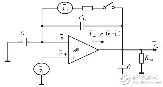
Figure 4 CTIA amplifier noise model
The noise voltage is
In this circuit, Cfb = 2 fF, Cpd = 1.3 pF, CL = 1 pf, α = 1.5, T = 300 K, then Vn = 2 mV.
3.3 Fixed Mode Noise (FPN)
It is called fixed-mode noise because the effect of this noise does not change with time, that is, the error expressed on each frame of the image is consistent. The fixed pattern noise of the pixel can be eliminated by the correlated double sampling circuit in the readout circuit. Through the above analysis, in this circuit, the main source of noise is the shot noise of the photodetector and the flicker noise of the CTIA amplifier, and the total output noise is
The noise voltage is
Where: Av is the output follower amplifier gain of 0.7.
According to the formula, the theoretical calculation of the noise voltage Vn = 3.1 mV, the actual circuit noise level will be about 2 times larger than the theoretical value.
4 Simulation and test results
4.1 Circuit layout and simulation results
The circuit designed in this paper uses CSMC's 0.5 μm CMOS process model to perform Spectre simulation, layout design and tapeout for the circuit.
Table 1 is the parameter setting of the detector, which is mainly determined by the equivalent resistance value and equivalent capacitance value of the detector made by the corresponding material and the photocurrent flowing through the detector, wherein Vref is added. The voltage at the positive phase of the amplifier.
Table 1 Value of unit circuit parameters during simulation
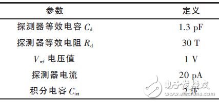
Figure 5 Simulation waveform of the CTIA output.
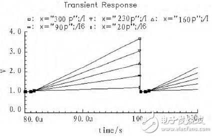
Figure 5 CTIA output waveform
As can be seen from Figure 5, when the signal current is 20 pA, the circuit output differential voltage is 90 mV. According to the estimated noise voltage, the signal-to-noise ratio of the minimum signal is SNR=15.
4.2 Test results
The circuit is streamed using CSMC's 0.5 μm standard CMOS process library. Table 2 compares the simulation results with the actual test results (Cf=20 fF, C1=150 fF, C2=18 fF signal input 20~300 pA, integration time) 20 μs).
Table 2 Comparison of simulation results and actual test results
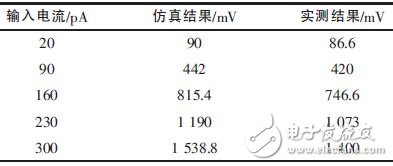
It can be seen from Table 2 that the measured result is slightly smaller than the simulation result. When the optical signal is 20 pA, the measured circuit noise voltage is 8 mV, and the SNR is 10.8.
5 Conclusion
In this paper, a high-gain, low-noise detector readout circuit is designed, which combines CTIA and CDS circuits to improve the integrated capacitance in the CTIA circuit, so that the circuit can read weak signals in a wide range and adopt switch control. And the CDS circuit to reduce noise and make the circuit signal-to-noise ratio reach 10, this circuit is of great significance for the design of the readout circuit of the low-light detection system in the aerospace field.
We cover many types of Connectors for industrial, electrical and automotive, such as IP68 and Waterproof Connectors, OBD diagnostic connectors, also the standard or custom-designed power connectors for MINI FIT, MICRO FIT, MATE-N-LOCK.
Connectors System,Board System Connector,Efi System Injector Connector,Efi System Car Connector
ETOP WIREHARNESS LIMITED , https://www.etopwireharness.com