
Design of high-precision open-loop tracking and holding circuit for time-interleaved ADC
0 OverviewWith the development of digital communication systems, high-speed digital processing systems require higher and higher conversions between analog and digital signals. At present, the two main development directions of high-performance analog-to-digital converters (ADCs) are high-speed, medium-low precision ADCs and low-speed, high-precision ADCs. Front-end T & H circuit is usually a key to ADC design, and its dynamic accuracy directly affects the performance of ADC.
1 Open loop T & H circuit
In the design of ultra-high-speed ADCs, generally a fully parallel Flash structure or a time-interleaved structure is used.
In the time-interleaved structure, the front-end T & H circuit can adopt an open-loop or closed-loop structure according to the design requirements. The closed-loop structure has a lower speed and higher accuracy, while the open-loop structure has a higher speed, but its accuracy is lower. The latter is used in this design.
The distortion of the T & H circuit mainly comes from the nonlinear MOS switch resistance, switch parasitic capacitance and switch charge injection. The distortion caused by the non-linearity of the on-resistance of the MOS switch when tracking the signal also limits the tracking and settling time of the circuit. Therefore, in ultra-high-speed T & H circuits, the input sampling switch must have a low and nearly constant on-resistance.
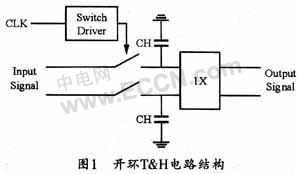
Figure 1 shows the structure of an open-loop T & H circuit. This circuit mainly includes three parts: a sampling switch, a sampling capacitor, and an output buffer. In order to solve the problem of poor linearity of the open-loop circuit itself, this paper uses bootstrap switch technology and reinforced buffer technology. The bootstrap sampling switch can improve the linearity of the on-resistance of the switch, and the differential structure can reduce the charge injection and improve the circuit performance; while the back-end enhanced buffer technology increases the bandwidth and gain, reduces the tube size and power consumption, and finally reaches The purpose of improving the accuracy of open-loop T & H circuits.
2 Bootstrap sampling switch
Since the sampling switch can be equivalent to a nonlinear resistance when it is turned on, it will introduce noise and nonlinear distortion. Therefore, the linearity of the sampling switch directly affects the accuracy of the T & H circuit. The high-linearity switches in current applications mainly include complementary MOS switches and bootstrap sampling switches.
Figure 2 shows the structure of the bootstrap sampling switch used in this article. The circuit mainly includes clock bootstrap and gate voltage bootstrap NMOS switch. Among them, M1 ~ M2 and C1 ~ C2 constitute the clock bootstrap circuit, M3 ~ M4 and CB constitute the gate voltage bootstrap circuit. The entire circuit is controlled by two phase non-overlapping clocks.

When the clock CLK is high, M6 ~ M7 is turned on to pull the gate voltage of the switch MS to ground, while M3 ~ M4 is turned on to charge the CB to Vdd; otherwise, when the clock CLK is low, the CB is discharged The M8 tube is turned on, the input signal voltage VIN is added to the lower plate of the CB, and the gate voltage of the switching tube MS is increased to (VIN + Vdd), so that the gate-source voltage of the switching tube is constant at Vdd.
In the traditional gate voltage bootstrap circuit, the parasitic capacitance of the upper and lower plates of the capacitor CB will cause charge sharing, thereby reducing the gate-source voltage of the switch. The gate-source voltage of the switch can be expressed as:
Among them, CP represents the sum of the parasitic capacitance connected to the charging capacitance CB. The addition of capacitor C3 can not only accelerate the rapid conduction of M9 tube, but more importantly reduce the parasitic capacitance of the circuit and reduce the impact on the input signal, thereby increasing the gate-source voltage of the switch MS and improving the linearity of the switch. The size of M1 ~ M4 can be appropriately larger to speed up the charging and discharging speed. In addition, the pull-down switch M2 can also be appropriately larger to accelerate the turn-off. Channel charge injection is another important factor that affects the linearity of the switch. Therefore, this design adds a redundant switch tube MD to reduce channel charge injection and improve the performance of the switch.
3 Buffer design
The buffer is another important part of T & H circuit design, and its gain and bandwidth will affect the dynamic performance of the entire ADC. In the previous open-loop structure, the structure of the buffer is mainly in the form of active follower (SF) and unity gain amplifier. The design structure of SF is simple and the power consumption is low. The ideal SF has good linearity and unity gain amplification capability and this performance is not related to bias current and transistor size. However, in practical applications, SF will be affected by the body effect and short-groove effect, resulting in signal attenuation and gain reduction. In order to improve the accuracy of SF, the transistor size and bias current can only be changed, but this contradicts the power consumption and speed of the circuit. In addition, another disadvantage of SF is that gain and linearity are not sensitive to design parameters, but this is also its advantage, and it is also insensitive to circuit mismatch.
Compared with SF, the gain of the unity gain amplifier itself is not unity gain, and needs to be obtained through design parameter adjustment. The more commonly used source-level weakened cross-coupled pair structure has a larger design margin than the ordinary differential pair structure and SF structure. According to the bandwidth requirements of this design, the load resistance cannot be too large. Therefore, in order to ensure the gain, the bias current and the tube size are relatively large, which affects the power consumption of the circuit. At the same time, in order to improve the voltage margin of the bias current tube and the input common mode range, a large source attenuation resistor must be introduced. The resistance will introduce noise and harmonics, affecting the dynamic accuracy of the circuit.
Through the analysis and comparison of the above two structures, combined with the design requirements for speed and power consumption, this article uses enhanced source follower technology to design a high-gain, high-bandwidth buffer that can meet the requirements of this design.
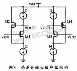
Figure 3 is the buffer structure used in this design. The P tube source follower is the main tube, and the N tube added on the basis of this source follower is used to clamp the source drain voltage of the P tube to make the drain source voltage constant. In the deep sub-micron process, the minimum channel length of the MOS tube will be reduced, the output resistance becomes smaller and is non-linear due to the short-channel effect and the back-gate effect, resulting in reduced circuit gain and the introduction of distortion. The N-tube can make the drain-source voltage of the main pipe constant, thereby reducing the short-channel effect, and also reducing the drain-source voltage of the P-tube, increasing the output resistance, thereby improving the gain and linearity. Compared with the traditional cascade source follower, the gate-drain capacitance is also reduced because the voltage at the drain terminal and the gate terminal keep almost the same voltage phase and amplitude, so the input capacitance will not increase but will decrease. The low input capacitance avoids attenuation of high-frequency input signals.
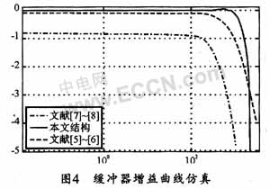
With reference to the pole-zero analysis, under the appropriate design parameters, due to the existence of the left half-plane zero, there is a process of upturn in the gain curve, thereby widening the buffer bandwidth. Figure 4 shows the buffered gain curve. From the gain simulation results of the three structures shown in Figure 4, it can be seen that the output buffer structure gain and effective gain bandwidth of this paper are significantly better than the other two structures under the same load.
4 Analysis of simulation results
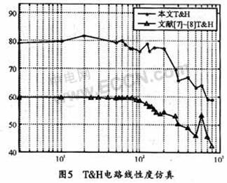
The circuit uses a 0.18μCMOS process model, the input signal peak-to-peak value is 1.6Vpp, and the sampling frequency is 400 MHz. It can be designed and simulated under HSPICE simulation conditions. Figure 5 shows the simulation results of the spurious-free dynamic range of the T & H circuit. It can be seen from the figure that the static accuracy of this T & H circuit structure is 79 dB, which is an improvement of nearly 20 dB relative to the 59 dB static accuracy of the cross-coupled structure. The dynamic accuracy of the circuit can reach 58.7 dB, a relative increase of 16.5 dB. It can be seen that the T & H circuit introduced in this article is better than the structural performance in the previous literature, whether it is static accuracy or dynamic accuracy, and it has also been reduced in terms of area power consumption.
5 Conclusion
In this paper, a 0.18 μm CMOS process is used to design a high-speed, low-power open-loop T & H circuit suitable for TI-ADC. Simulation results show that the accuracy of the open-loop T & H circuit can be significantly improved by using high linearity bootstrap switches and high-gain high-bandwidth output buffers. At a sampling frequency of 400 MHz, an input signal range of 1.6 Vpp, and a signal input frequency of 799.8047 MHz, the approximate accuracy of 9.5 bits is finally obtained, while the circuit power consumption is only 10.56 mW. It can be seen that the design of this open-loop T & H circuit is simple and the power consumption is low, which can better meet the application requirements of higher linearity.
XRX using the advanced technology and equipment , manufacturing the best quality fiber connector for all our customers, It is a kind of insert an extraction connector based on the single core plug and adaptor, which both ends of optical cable have the connector plugs, according to the joint can be classified to type SC,FC,LC,ST,MU,MPO,MTRJ,E2000,and so on ,according to difference of the end face have the type PC,UPC,APC and so on. SC stands for Subscriber Connector- a general purpose push/pull style connector. It is a square, snap-in connector latches with a simple push-pull motion and is keyed.
SC Patch Cord,SC SC Patch Cord,SC Fiber Patch Cable,SC Fiber Cable
Chengdu Xinruixin Optical Communication Technology Co.,Ltd , https://www.xrxoptic.com