
1 Introduction
The open multimedia application platform OMAP5910 is a unique dual-core architecture that combines a high-performance, low-power TMS320C55x DSP core with a highly controlled ARM925 microprocessor for the comprehensive processing power of portable handheld devices. ARM is longer than control, DSP is longer than algorithm, but in order to coordinate the two to produce the greatest overall performance, communication technology research between dual core is essential.
2 Introduction to the dual-core structure of OMAP5910
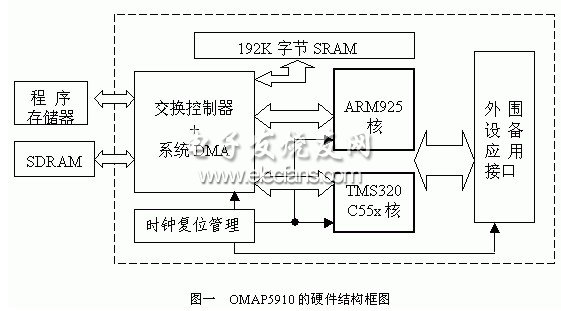
As shown in Figure 1, the dual-core architecture of the OMAP5910 includes enhanced ARM925 core, TMS320C55x DSP core, switching controller, system DMA controller, clock reset management module, internal SRAM and external device application interface.
The enhanced ARM925 core is an advanced 32-bit reduced instruction set computer processor that operates at 150 MHz and can execute 32-bit or 16-bit instructions to process 32-bit, 16-bit, and 8-bit data. As the host of the OMAP5910, the ARM925 can access up to 4G of space.
The TMS320C55xDSP core operates at 150Mhz and has 32K words of DASRAM, 48K words of SARAM, 16K words of ROM and 12K words of high-speed instruction cache memory. There are also memory management units for address translation, two-level interrupt managers and other modules. The function is very powerful, but the power consumption is quite low, which is the most power-saving in the current TMS320 DSP family.
The switch controller is mainly used to provide asynchronous operations of the OMAP5910 system storage resources (including 192K bytes of internal SRAM, 64M bytes of external SDRAM, and 128M bytes of external FLASH) for ARM, DSP, and system DMA. The system DMA controller is designed with low power consumption, supports 8-bit, 16-bit, 32-bit data transmission between external memory, ARM925 and peripherals, and has functions such as burst transfer and data packing.
The clock reset management module can flexibly set and manage the clocks of the ARM part, the DSP part, and the switch controller, so that each unit can work in different power saving modes, thereby minimizing the power consumption of the entire system.
The internal 192K byte 32-bit data width SRAM provides large data and code storage space for applications such as liquid crystal displays. The peripheral device application interface provides convenience for the OMAP5910 to connect the LCD, camera, air interface, USB, etc. off-chip.
3 OMAP5910 dual-core communication mechanism
The OMAP5910 supports communication between internal dual cores in three ways. The first way is through the dual-core shared mailbox register Mailbox, which can interrupt each other and pass a small amount of data through the mailbox register. The second way is that ARM obtains access to the DSP memory space and I/O space through the host interface, and then ARM transfers the data between the dual cores. The third way is to map the external storage space of the DSP to the OMAP5910 system storage resource through the setting of the DSP memory management unit by ARM, and the data transfer between the dual cores is completed by the DSP.
The three communication methods have their own advantages. The first method transmits a small amount of data, but the information is reliable and timely, which is very suitable for completing the handshake in dual-core communication. The latter two modes are suitable for transferring large amounts of data between dual cores, but the controllers of data transmission are different. The second mode is controlled by ARM, and the third mode is controlled by DSP. In some relatively complex applications, ARM is often busy with control of many peripheral devices, and there is no more time to complete data transfer between dual cores. In this case, the third way to complete data movement is inevitably the most ideal choice. Based on this consideration, an introduction to the third method will be given below.
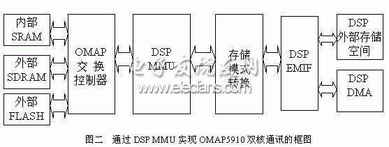
3.1 Principle Block Diagram
The essence of communication between the dual core through the memory management unit MMU of the DSP and the external memory interface EMIF is to use the DSP MMU to map the external memory of the DSP on the internal SARAM, external SDRAM and FLASH of the OMAP5910, so that ARM, DSP and DSP DMA can access. These three storage areas thus enable data sharing. The block diagram is as follows:
132Kv Transformer,132Kv Power Transformer,132Kv Power Transformer With Oltc,132Kv Transformer With Oltc
Hangzhou Qiantang River Electric Group Co., Ltd.(QRE) , https://www.qretransformer.com