
Why does the threshold voltage of E-MOSFET increase with the increase of doping concentration of semiconductor substrate? And as the temperature rises, it drops?
The threshold voltage of the E-MOSFET is the gate voltage required to generate an inversion layer (conducting channel) on the semiconductor surface. For n-channel E-MOSFETs, the semiconductor surface can be considered strongly inversion when the gate voltage causes the surface energy band of the p-type semiconductor to bend down to a surface potential ψ ≥ 2ψB, because at this time the minority carriers in the inversion layer. The (electron) concentration is equal to the majority carrier concentration (~doping concentration) in the body; ψB here is the semiconductor Fermi potential, which is the difference between the semiconductor forbidden band center and the Fermi level. The threshold voltage VT consists of three parts of voltage (regardless of the offset voltage): the voltage drop Vox across the gate oxide; the voltage drop near the semiconductor surface 2ΨB: the voltage drop that counteracts the effects of various charges in the MOS system - flat band Voltage VF.
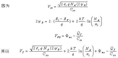
In the expression of the threshold voltage, the factor related to the doping concentration and temperature is mainly the semiconductor Fermi potential B. When the doping concentration NA of the p-type semiconductor substrate increases, the semiconductor Fermi level tends to change at the valence band top, and the semiconductor Fermi potential B increases, thereby making it more difficult to achieve the inversion layer production condition of ψs≥2ψB, so The threshold voltage increases.
When the temperature T rises, the semiconductor Fermi level will tend to change in the band gap center, then the semiconductor Fermi potential B will decrease, resulting in more easily reaching the inversion layer generation condition of ψs≥2ψB, so the threshold voltage decreases.
(2) Why does the source-drain current of the E-MOSFET become larger and saturated after the pinchoff (ie, independent of the source-drain voltage)?
[Answer] The channel pinch off of the E-MOSFET is a state where the gate voltage exceeds the threshold voltage and the channel is present, and the source-drain voltage causes the channel to pinch off at the drain terminal. In fact, the channel being pinched at one end does not mean that there is no channel at all. When the gate voltage is less than the threshold voltage, there is no channel at all, which is a non-conducting state-off state. Since the pinch-off region of the channel is a depletion region, and the increased source-drain voltage also mainly falls in the pinch-off region, there is a strong electric field in the pinch-off region, as long as carriers reach the edge of the pinch-off region. It can be pulled by the electric field and output from the drain, so the pinch-off area not only does not prevent the passage of carriers, but on the contrary can conduct electricity well, so there is a channel and the channel is pinched at one end. It is a very good conductive state, then the output source-leakage current is maximum after the pinchoff.
After the channel of the E-MOSFET is pinched off at the drain terminal, since the pinch-off region is basically a depletion region, the source-drain voltage further increased, that is, will mainly fall in the pinch-off region, and thus the pinch-off region is not pinched off. The channel—the length of the remaining channel remains essentially the same; and the source-drain current after pinchoff is mainly determined by the length of the remaining channel, so the source-drain current is basically Does not vary with source-drain voltage - the output current saturates.
(3) Why is the saturation source-drain current of a short-channel E-MOSFET not fully saturated?
For short-channel MOSFETs, there are basically two causes of saturation of the output source-drain current: one is the saturation of the current due to channel pinchoff; the other is the saturation of current caused by the saturation of the current.
For the saturation of the channel pinch off, because the length of the pinch-off region increases with the voltage on it, the length of the remaining channel will also decrease with the source-drain voltage. This can cause the source-drain current to increase correspondingly with the source-drain voltage—the output current is not fully saturated. However, the degree of current saturation is related to the channel length: For long-channel MOSFETs, the length of the pinch-off region varies with the source-drain voltage and is negligible with respect to the entire channel length. The source-drain current after a pinch pinchoff is approximately “saturatedâ€; however, for a short-channel MOSFET, this pinch-off region length varies with the source-drain voltage and cannot be compared with the entire channel length. Ignored, so the source-drain current after the pinch-off of the channel will obviously increase with the increase of the source-drain voltage-not saturation.
For the saturation of current caused by the saturation of the current, in general, when the electric field is very strong and the carrier velocity is saturated, further increase of the source-drain voltage will not increase the current. Therefore, the saturation current at this time is in principle independent of the source-drain voltage.
For short-channel MOSFETs, there is also an important cause of current unsaturation, the so-called DIBL (drain induced source terminal barrier lowering) effect. Since there is always a barrier caused by a high and low junction between the source region and the channel, the higher the source-drain voltage, the lower the potential barrier, and the larger the source-drain current through the channel. The output current does not saturate.
In short, the factors leading to the unsaturation of the short-channel MOSFET current are the channel length modulation effect and the DIBL effect.
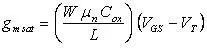
(4) Why does the saturation source-drain current of the E-MOSFET have a square relationship with the saturation voltage?
[Answer] The saturation source-drain current expression of the enhanced MOSFET (E-MOSFET) is
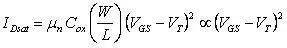
The saturation voltage (VGS-VT) is the source-drain voltage at the pinch-off of the channel. The relationship between the saturation source-drain current IDsat and the saturation voltage (VGS-VT) of the E-MOSFET appears as a parabola on the transfer characteristic (IDsat-VGS) curve of the MOSFET. There are two reasons for this squared relationship:
The larger the 1 channel width, the higher the saturation source-drain current and the higher the saturation voltage.
2 Current saturation corresponds to channel pinchoff, and the pinch-off region is the depletion layer. There is a square root relationship between the width and the voltage, which leads to the above squared result. Because MOSFETs have such a squared current-voltage relationship, they are often referred to as square-rate devices.
(5) Why does the saturation MOSFET's saturation source-drain current have a negative temperature coefficient?
[Answer] The MOSFET saturation source-leakage current can be expressed as

In this relationship, because the material parameters and the device structure parameters are not related to the temperature, the temperature-related factors are mainly two: the threshold voltage VT and the carrier mobility μn.
Since the threshold voltage VT of the MOSFET has a negative temperature coefficient, as the temperature increases, the saturation source-drain current of the MOSFET output increases, which results in the current having a positive temperature coefficient.
The carrier mobility, μn, will generally decrease with increasing temperature near room temperature (mainly due to lattice vibration scattering):
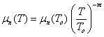
In the formula, To=300K, m=1.5 to 2.0. This temperature characteristic of the mobility leads to the gain factor of the MOSFET.
It also has a negative temperature coefficient. Thus, as the temperature increases, a decrease in the mobility causes the output source-drain current of the MOSFET to decrease, that is, the current has a negative temperature coefficient.
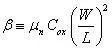
The different effects of the above two factors, the threshold voltage and the carrier mobility, can be known from the expression of the MOSFET saturation current:
1 When the saturation voltage (VGS-VT) is large (ie, VGS-VT), the effect of the threshold voltage temperature relationship is negligible, and the temperature characteristics of the output source-drain current will be mainly determined by the temperature dependence of carrier mobility. , ie having a negative temperature coefficient (temperature rise, IDS drop);
2 When the saturation voltage (VGS-VT) is small (that is, VGS-VT), the temperature characteristics of the output source-drain current will mainly depend on the temperature relationship of the threshold voltage, and thus have a positive temperature coefficient (temperature rise, IDS Also increase).
For the general MOSFET, in order to obtain a large transconductance, the saturation voltage (VGS-VT) is often chosen to be larger, so the influence of the threshold voltage may not be considered, and thus the saturation source-drain current usually has a negative temperature coefficient. . Therefore, the general MOSFET has a certain self-protection function, you can directly connect multiple die together, and will not appear due to uneven current distribution caused by failure; use this method of parallel die can It is convenient to increase the output current of the device (in fact, power MOSFETs use this measure to achieve high current).
(6) Why is the transconductance in the saturation region of the MOSFET larger than the transconductance in the linear region?
[Answer] Both the saturated zone and the linear zone show the state of the channel, but their fundamental difference is whether the channel is pinched. The effect of voltage on the channel width is that the gate voltage will cause the channel width to change uniformly, and the source-drain voltage will cause the channel width to vary unevenly (causing the channel to first pinch off at the drain terminal).
In the linear region, since the source-drain voltage is low, the width of the entire channel does not change much from beginning to end. In this case, the gate voltage controls the channel conduction capability to be relatively poor, and thus the transconductance is small. At the same time, as the source-drain voltage increases, the variation of the channel width increases, so that the channel width at the drain end becomes smaller, the gate voltage controls the channel conductivity and the transconductance increases.
In the saturation region, the source-drain voltage is higher and the channel pinch off, that is, the channel width at the drain end is 0, so the gate voltage controls the channel's ability to conduct electricity (small gate voltage can be Control the conduction and stop of the channel, so the transconductance at this time is very large. Therefore, the transconductance in the saturated region is greater than that in the linear region.
It can be seen that the closer the channel is to the pinch off, the stronger the control capability of the grid is, and the larger the transconductance is. After the channel is completely pinched and the current is saturated, the transconductance reaches the maximum—saturated transconductance.
(7) Why is the MOSFET saturation transconductance generally proportional to the saturation voltage? But why is it sometimes inversely proportional to the saturation voltage?
[Answer] 1 When the source-drain voltage VDS is certain: the saturation current IDsat of the E-MOSFET differentiates the gate voltage, and the saturation transconductance gmsat is proportional to the saturation voltage (VGS-VT):
This proportional relationship derives from the fact that the higher the saturation voltage, the more difficult it is for the channel to pinch off, and the thickness of the conductive channel must be greater. Therefore, the output source-drain current at the same gate voltage is higher. Larger, so the greater the transconductance.
2 When the saturation current IDsat is fixed: the saturation transconductance gmsat is inversely proportional to the saturation voltage (VGS-VT):
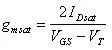
This is because the higher the saturation voltage, the more difficult it is for the channel to be pinched off, and the smaller the control capability of the gate, that is, the smaller the transconductance.
In short, when the source-drain voltage is constant, the saturation transconductance is proportional to the saturation voltage, and when the source-drain current is constant, the saturation transconductance is inversely proportional to the saturation voltage.
This inverse proportional relationship exists in other cases, such as the relationship between power consumption P and resistance R: When the current is constant, the power loss is proportional to the resistance (P=IV=I2R); when the voltage is constant, the power consumption It is inversely proportional to the resistance (P=IV=V2/R).
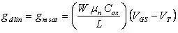
(8) Why does the MOSFET linear region source-drain conductance equal the transconductance of the saturation region (gate transconductance)?
[Answer] The source-drain conductance gdlin of the linear region of the MOSFET and the gate transconductance gmsat of the saturation region are performance parameters that characterize the voltage-to-channel conductance, ie, the ability to control the source-drain current.
In the linear region, the channel is not pinched, but the source-drain voltage will make the channel width non-uniform; at this time, the source-drain voltage changes, the source-drain conductance gdlin means that the channel is not pinched, The source-drain voltage controls the source-drain current. This control is effected by the nonuniform variation of the channel width.
The gate transconductance-saturated transconductance gmsat in the saturation region is the characteristic of the gate-source voltage controlling the source-drain current in the case of channel pinch-off. At this time, the width of the remaining channel is not uniform. , this control is also equivalent to the effect of non-uniform changes in the channel width, so the gate transconductance at this time is equivalent to the source-drain conductance of the linear region:
(9) Why is the saturation-region current and then the linear-region current appearing first in the gate-to-drain transfer characteristics of the E-MOSFET, as the gate-source voltage increases?
[Answer] The gate-drain transfer characteristic of the E-MOSFET is shown in Figure 1. When the gate-source voltage VGS is less than the threshold voltage VT, the device is off (no channel) and the source-drain current is small (referred to as subthreshold current).
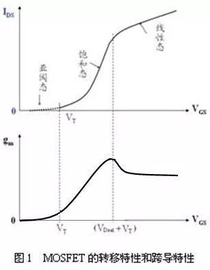
When VGS > VT, a channel appears, but if the source-drain voltage VDS = 0, no current will be generated; only when VGS> VT and VDS> 0, the current will be generated, then there must be VDS> (VGS -VT), so the MOSFET is in the saturation state of the pinchoff, so the source-drain current squares up with the gate-source voltage. Correspondingly, the saturation transconductance increases linearly with the gate-source voltage due to the fact that the saturation transconductance is proportional to the saturation voltage (VGS-VT).
When the gate-to-source voltage further increases so that VDS<(VGS-VT), the MOSFET will turn into a linear operating state where the channel is not pinched, and the source-drain current increases linearly with the gate-source voltage. Big. At this time, the transconductance no longer changes (regardless of the gate voltage).
(10) Why is the cutoff frequency fT of the MOSFET current amplification factor proportional to the transconductance gm?
[Answer] The fT of the MOSFET is the frequency at which the output current drops to equal the input current as the frequency increases. The greater the transconductance gm of the device, the greater the output current, the slower the output current decreases with frequency, and the larger the cutoff frequency, ie, the relationship between fT and gm:
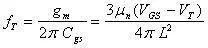
Due to the proportional relationship between fT and gm, there is also a positive relationship between fT and the saturation voltage (VGS-VT), so that higher frequencies require a larger saturation voltage.
(11) Why is there a conflict between increasing the MOSFET frequency and increasing the gain?
[Answer] The high frequency of the MOSFET requires it to have a large transconductance, but in the case of a certain source-drain voltage, the larger transconductance requires that it have a larger saturation voltage (VGS-VT), so the high frequency It also requires a larger saturation voltage.
Since the voltage gain of the MOSFET is a derivative of the output voltage VDS versus the gate-source voltage VGS with a constant source-drain current, the saturated-state voltage gain Kvsat will require the device to have a smaller saturation voltage (VGS-VT):

This is because when the IDsat is fixed, the saturation voltage is lower and the saturation transconductance is larger, so the Kvsat is also larger.
It can be seen that increasing the frequency and increasing the voltage gain have contradictions in the requirements for the saturation voltage of the device. Therefore, when the operating current IDsat is constant, in order to increase the voltage gain, (VGS-VT) and the channel length L should be increased. This consideration has important implications for high-gain MOSFETs; however, this reduction (VGS-VT) considerations are detrimental to increasing the cut-off frequency.
(12) Why is there a “threshold loss†in the MOS diode formed by the gate-source short circuit of the E-MOSFET?
[Answer] The connection of this integrated MOS diode and its volt-ampere characteristics are shown in Figure 2. Because the gate and drain are shorted, VGS=VDS. Therefore, when the voltage is small (VGS=VDS
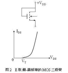
Due to VGS=VDS, the output volt-ampere characteristics of this diode will exactly match the transfer characteristics. Because there is a square relationship between the saturated output current IDsat and the saturation voltage (VGS-VT) of the MOSFET, the output volt-ampere characteristic of the diode at VGS=VDS≥VT is a parabolic relationship, and this is also the relationship of its transfer characteristics.
The so-called threshold loss, for example, in the gate circuit, is a phenomenon in which the output high level is lower by one threshold voltage than the power supply voltage. The volt-ampere characteristics of an E-type, gate-drain short MOS diode can be seen. When the output source-drain current IDS is reduced to zero, the source-drain voltage VDS is reduced to VT accordingly. This means that the output voltage of such a diode can only fall to VT, and cannot be reduced to zero. This "voltage-free, current-free" nature of the integrated MOS diode used as an active load will inevitably cause a threshold loss.
(13) Why does BJT exist in the MOSFET? What is the danger of this effect?
[Answer] 1 For a conventional MOSFET: As shown in Figure 3(a), the source, drain, and p-substrates constitute an npn parasitic transistor. When the electric field in the channel is strong, the electrons in the vicinity of the pinch-off region are about to get a lot of energy and become hot electrons, and then these hot electrons, through collision and ionization with the valence electrons, will form an empty flow to the substrate. The hole current Ib; the over-substrate current is the base current of the parasitic transistor. When the thermal electron effect is serious and the substrate current is large, the parasitic transistor can be turned on, thereby destroying the performance of the MOSFET. The adverse effects of this hot electron effect are often an important failure mechanism for shorter channel MOSFETs.
2 For CMOS devices: In the CMOS device chip, there are four layers of npnp structure - thyristors. When the BJT is turned on due to the hot electron effect, the so-called "latch-up effect" can occur, resulting in device failure.
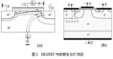
3 For VDMOSFET: Observe the structure in Figure 3(b). It can be seen that when the device is conducting forward, there is a parasitic npn transistor operating in an amplified state (the n+ source region is the emitter region, and the n- epitaxial layer is the epitaxial region. Electrical area, p-channel is the base area). The possible conductive path of the parasitic transistor is in parallel with the ID of the MOSFET, so when the VDMOSFET is operating, care must be taken to prevent the parasitic transistor from turning on; otherwise, the continuity of the parasitic transistor may cause secondary breakdown, making the power MOSFET completely lose the capacity of.
In order to avoid the VDMOSFET operating in the forward direction, in which the parasitic npn transistor is turned on, it can be tried to make the current amplification coefficient of the parasitic transistor become very small, even to zero - using "cathode short circuit technology", that is, the parasitic transistor The emitter is shorted to the base and the process is achieved by extending the metal electrode of the emitter region (source region) to the surface of the channel body region. Since this cathode short-circuit structure blocks the function of the emitter-injected carriers, the conduction of the parasitic transistor can be prevented.
For the VDMOSFET, after the cathodic short-circuit structure is adopted, a pn-n+ diode is actually formed inside the device. This diode is inversely connected in parallel with the VDMOSFET, which also conveniently places a damper diode in the VDMOSFET ( Freewheeling diode) This diode plays an important role in discharging reverse electromotive force and preventing breakdown of the body transistor.
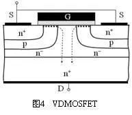
(14) Why is there a role of JFET in VDMOSFET? What are the adverse effects?
[Answer] As shown in Figure 4, the source-drain current flows downward from the chip surface and is a pn junction on both sides of the current path. Therefore, this process of current transport is quite equivalent from the working principle. So a parasitic JFET. This allows the VDMOSFET to be used as a series combination of a MOSFET and a parasitic JFET, where a large portion of the n-drift region is equivalent to the parasitic JFET channel.
Since the output AC resistance of the JFET is very large, and because of the high source-drain voltage, it also has a large output DC resistance, so the on-resistance of the VDMOSFET is greatly increased, so the thickness and doping concentration of the n-drift region The overall device performance has a greater impact.
In order to eliminate the influence of the parasitic JFET in the VDMOSFET, in order to reduce the on-resistance, it is necessary to change the structure, and thus a MOSFET having a V-shaped trench gate, a U-shaped trench gate, and a trench gate is developed.
(15) Both IGBTs and MCTs are MOSFET-controlled power field effect transistors. Why are they two completely different devices?
[Answer] The common points of IGBT (Insulated Gate Bipolar Field Effect Transistor) and MCT (MOS Control Thyristor) are:
1 is a MOS gate controlled device, it has the advantages of power field effect transistors;
2 In the structure, there are four-layer and three-junction thyristor structures, so the anode current latch-up effect will occur under certain conditions.
3 All of them can adopt a structure in which multiple cells are connected in parallel, so a large working current can be obtained.
3 All of them are devices with two carriers participating in the work. Therefore, they are all bipolar field-effect transistors. The on-resistance is low, but the switching speed is relatively lower than that of MOSFETs.
The biggest difference between IGBTs and MCTs is that they have different operating states and properties, so they are two completely different devices:
The operating current of the IGBT is mainly the current through the MOS channel, and the thyristor current therein needs to be avoided as much as possible (the maximum operating current of the IGBT, ie, the current at which the thyristor does not conduct), and therefore, essentially, IGBT is basically a kind of MOSFET, so IGBT has many advantages of MOS device, such as stronger gate control ability and lower driving power (because of large input resistance and small input capacitance) .
MCT and IGBT, on the contrary, its operating current is mainly thyristor current, as MOS channel current, it is mainly to trigger the thyristor conduction or off role, not MCT's main operating current, so essentially Look, MCT is basically a thyristor - bipolar device, so MCT has the advantages of low on-resistance, high withstand voltage, and large power capacity.
Although 2 IGBTs are essentially MOS devices, they are different from ordinary MOSFETs because IGBTs have minority carriers injected into high-resistance voltage-resistant layers (drift regions) during conduction operation, which can generate conductivity modulation. Its on-resistance is smaller, the current capacity of the device is increased (the current density is 2 to 3 times higher than that of the VDMOSFET); at the same time, the operating voltage is increased due to the introduction of a high-resistance and pressure-resistant layer. Therefore, the power capacity of the IGBT is large. Only the switching speed of the IGBT is correspondingly reduced due to the introduction of minority carriers.
3 Although the MCT is essentially a thyristor, and the MOS gate can shut off the anode current, the MCT is different from a normal turn-off thyristor (GTO). Because MCT is actually a composite device combining a unipolar MOSFET and a bipolar thyristor, it is also a so-called Bi-MOS device, so it has the advantages of both MOS devices and bipolar devices. : Stronger gate control capability, lower drive power, higher switching speed, higher power capacity.
Lithium Battery,Lithium Batteries,Lithium Car Battery,Lithium Cell
SUZHOU DEVELPOWER ENERGY EQUIPMENT CO.,LTD , https://www.fisoph-power.com