
Driven by the current communication market, communication technology is advancing rapidly, and handheld wireless communication terminals have become one of the popular applications. Therefore, monolithic integrated RF transceiver systems are receiving more and more attention. A typical RF transceiver system consists of a low noise amplifier (LNA), a mixer (Mixer), a filter, a variable gain amplifier, and a unit of the frequency synthesizer required to provide the local oscillator, as shown in Figure 1. For circuit systems operating in the RF environment, such as 2.4G or 5G WLAN applications, the system should include a small signal noise sensitive circuit for the RF front end, a module with high linearity requirements for the baseband low frequency large signal, and a PA with high current at the transmitting end. Modules, digital blocks in phase-locked loop frequency synthesizers, and VCOs with non-linear characteristics. Numerous circuit units and their rich features necessarily require a feature-rich and powerful design platform in the design of such systems. After a comprehensive comparison, this article selected the Cadence Virtuoso full custom IC design tool.
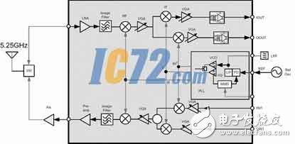
Figure 1 Typical RF Transceiver System
Virtuoso is Cadence's professional software for analog/digital hybrid circuit simulation and RF circuit simulation. Based on this platform, Cadence has also developed new technologies for RF design, including RF extraction technology and two new design flows for wireless chip design. Not only that, but Virtuoso has integrated technology from partners Agilent, CoWare, Helic and Mathworks, and its RF design capabilities have been greatly enhanced. With this new technology, design duplication can be reduced and time to market can be reduced. Its AMS tools enable top-down, digital-to-analog hybrid circuit design; Composer tools make it easy to enter and manage circuit designs; Spectre/SpectreRF simulators are highly accurate and suitable for different circuit designs; Layout tools include Layout, cross-reference, routing, layout verification, parameter extraction and more; in addition, Virtuoso enables reliable post-simulation and yield control.
Virtuoso-based behavioral simulation and system planning
The final success of the design of the RF transceiver system, and whether the module index allocation is reasonable and feasible depends on the behavior and modeling of the system before the specific circuit design, so-called behavior simulation. This is also a key step in the top-down design pattern. Cadence's built-in Verilog-A and VHDL simulators, as well as simulation methods for mixed input modes, offer this possibility. Moreover, Cadence software provides a large number of behavior models for free use. For RF system design, all that is required is to call and set the expected index requirements of each module, and the behavior characteristics of the system can be obtained quickly through simulation. According to the requirements, the indicators of each module can be easily re-simulated until the behavior of the system meets the requirements. Taking the receiver as an example, the receiving system is shown in Figure 2. The indicator settings for each module are very specific, such as input and output impedance, gain, isolation, noise figure NF, linearity IP3, DC offset IP2, and so on. After the simulation is completed, the indicator assignment tasks for each module are also completed at the same time.
After each module is implemented by a specific circuit, the corresponding design module can be replaced one by one to perform system simulation. It can be seen whether each module satisfies the needs of the system, and then evaluates the impact of each actual module on system performance.
Circuit module based on Virtuoso Spectre/SpectreRF
Simulation design
Based on the above behavior simulation results and indicator assignment results, the system module design tasks can be divided, and each unit block is separately designed and simulated.
LNA
The LNA is an active component at the forefront of the RF receiver that determines the noise performance of the system. The requirements are mainly to have as low a NF as possible and sufficient power gain, good input matching, followed by high linearity and isolation. Its circuit is shown in Figure 3. NF analysis can be performed using Spectre's SP analysis or SpectreRF's PSS+Pnoise analysis. The results of NFmin can also be used to select the size of the transistor so that the optimal source impedance meets the minimum noise requirements.

Figure 2 LNA circuit schematic
Mixer
The mixer is the core of the transceiver. Since the conversion is done, the main simulation method requires the SpectreRF simulator. The gain, NF, etc. of the mixer are related to the input and output, but the input and output work in different frequency bands. Other analysis is often performed on the basis of PSS analysis to get correct results, such as PSP, Pnoise, PAC, etc. The structure of the mixer is a typical double-balanced Gilbert.
VGA
Baseband VGA has low noise and high gain, so it has low requirements on noise. It mainly requires high linearity and gain. SpectreRF's PSS scan can easily scan the input of the module and automatically scan the curve. Extend, directly indicate the intersection position and numerical value of the linearity P1dB and IIP3, which is very convenient and intuitive. This method is more flexible and efficient than the traditional two tone test. The simulation of the IIP3 indicator of the VGA in different gain states requires only the control to be written as a variable, and the value of the scan variable can be done in the ADE environment. The results obtained can be conveniently compared and analyzed. The ideal VGA circuit can be obtained by adjustment. You can even save various settings under ADE as ocean script files. With the automatic operation of scripts, Cadence can automatically complete simulations and save data results as long as various simulation tasks are scheduled in advance. After comparing and analyzing the data, the performance of the circuit can be learned, and as a guide to the gradual improvement, a circuit module that satisfies the needs of the system can be obtained.
PLL module
The simulation of each module of the PLL is a challenging task. The PLL itself is a digital/analog hybrid module, but each module is generally designed in an analog manner. The simulation of the PLL includes testing of hundreds of metrics that use almost all of Spectre and SpectreRF's simulation tools. Taking the simulation of VCO and CP as an example, the nonlinear characteristic of VCO determines that its noise calculation cannot be performed in a small signal manner. PSS+Pnoise can accurately simulate the phase noise performance of VCO. The frequency tuning gain Kvco of the VCO can be obtained by scanning.
The charge pump output current characteristic is a common curve for measuring CP performance, and CP determines the gain and in-band noise performance of the PLL loop. The constant current and matching characteristics of the current source of the CP under different states can also be easily obtained by scanning.
The above is the circuit design simulation process of several typical unit modules of the RF receiver. The simulation of each unit block of the system can be simultaneously developed, and the completed module can be substituted into the behavior system at any time to verify the design result. After several iterations of modification and verification, the receiving system that meets the requirements can be finally obtained.
Temperature analysis
To ensure the reliability and yield of the final system design, a critical step is to analyze the temperature and extreme conditions in the design of each unit block. These features can be performed in Cadence Virtuoso by setting different simulation temperatures, by setting the Corner settings of the simulation model, and directly using the Monte Carlo simulation tools provided.
Overall circuit simulation of RF transceiver system
After each module circuit design verification is completed, all modules can be connected into the system, and PAD, ESD, etc. are combined to form a complete chip system, as shown in Figure 4. Simulate testing of this system with excitation, as shown in Figure 5, can simulate the entire system circuit. If the hardware resources used in the simulation calculation are large enough, the system can directly perform tran, SP, PSS, and PSP, Pnoise, PAC analysis, etc., to obtain the performance of the entire chip. If the resources are insufficient, you can consider grouping and partitioning the functions by function. Since the separated blocks are relatively independent, the characteristics of the overall system are not much different from the block simulation.
Layout design and post simulation
The layout design of each module can be started on the basis that the design indicators of each module meet their own and system requirements, as shown in Figure 6. First of all, the Layout-XL component loading function can be used to directly transfer the layout components from the schematic to perform the rough layout of each module, mainly to arrange the connection ports with other modules and the pre-layout of some important components. Then pre-layout all modules from the system for overall layout considerations. With the hierarchical management and operation features of the Virtuoso Layout tool, you can systematically consider the placement of each module and its interface with other modules.
Figure 3 Single-chip RF transceiver chip layout design
After the system is laid out, boundary conditions are assigned to each module. The boundary conventions are adhered to during the separate layout of the module. After the layout has reached a certain stage, it can be transferred to the system layout to check, and make necessary adjustments at any time to meet the specific conditions of each module.
The specific layout of the Virtuoso layout tool can be fully utilized, such as the full use of shortcut keys to make the layout design smooth and efficient; use Layout-XL cross-reference to find the wrong connection or inadvertent short circuit at any time; DRD's real-time rule checking avoids most layouts that violate design rules.
The rule check of the layout can use Virtuoso's Diva tool, and DRC, LVS, Extract, etc. can be done in a friendly interface. For the small size of the RF circuit layout components, it is appropriate to use Diva to do most of the work. If you want to further improve the accuracy of layout extraction and post-simulation, consider using the Assura tool.
10 inch tablet is the most important size on tablet market. Which kind of clients like more? The answer is loving bigger size or storage, longer working time, etc. Since Android Tablet 10 inch is usually equipped with full HD screen, memory support up to 8GB, storage up to 256GB, battery up to 7000mAh-working 5-8hours. However, 8 inch android tablet mainly up to 4GB ram 64GB ROM, 4000mAh battery. At this store, you can see more than ten different 10 inch tablets on sale and one 10 inch windows tablet with magnetic keyboard option, and high level CPU and SIM Card option. Besides, you can also see amazon tablet 10 inch with competitive cost, especially take above 1000pcs. Except android tablet, 14 inch 64Gb Student Laptop for online learning, 15.6 inch celeron n5095 business laptop, 15 inch intel i3, i5, i7 10th or 11th generation Gaming Laptop and 16 inch laptop with 4gb graphics card and 16gb ram 512GB ssd alternatives also.
Any other special requirements, just fee free to contact us. Will try our best to support you.
10 Inch Tablet,10 Inch Tablets On Sale,Android Tablet 10 Inch,Amazon Tablet 10 Inch,10 Inch Windows Tablet
Henan Shuyi Electronics Co., Ltd. , https://www.shuyilaptop.com