
Guide:
Integrating GaN FETs with their drivers improves switching performance and simplifies GaN-based power stage designs.
Gallium nitride (GaN) transistors have a much faster switching speed than silicon MOSFETs, making it possible to achieve lower switching losses. However, when the slew rate is high, the specific package type limits the switching performance of the GaN FET. Integrating GaN FETs and drivers in a single package reduces parasitic inductance and optimizes switching performance. The integrated drive also provides protection.
Introduction
Gallium nitride (GaN) transistors have better switching performance than silicon MOSFETs because of the lower on-resistance of gallium nitride (GaN) transistors with the same on-resistance and avoiding reverse recovery caused by body diodes. loss. Because of these characteristics, GaN FETs can achieve higher switching frequencies, while maintaining reasonable switching losses while increasing power density and transient performance.
Traditionally, GaN devices have been packaged as discrete devices and driven by separate drivers because GaN devices and drivers are based on different processing techniques and may come from different vendors. Each package will have bond wires and leads that introduce parasitic inductance, as shown in Figure 1a. These parasitic inductances can cause switching losses, ringing, and reliability issues when switching at high slew rates of tens to hundreds of volts per nanosecond.
Integrating a GaN transistor with its driver (Figure 1b) eliminates the common source inductance and greatly reduces the inductance between the driver output and the GaN gate, as well as the inductance in the driver ground. In this article, we will examine the problems and limitations caused by package parasitics. Optimizing these parasitic effects in an integrated package reduces this problem and achieves excellent switching performance at high slew rates above 100V/ns.
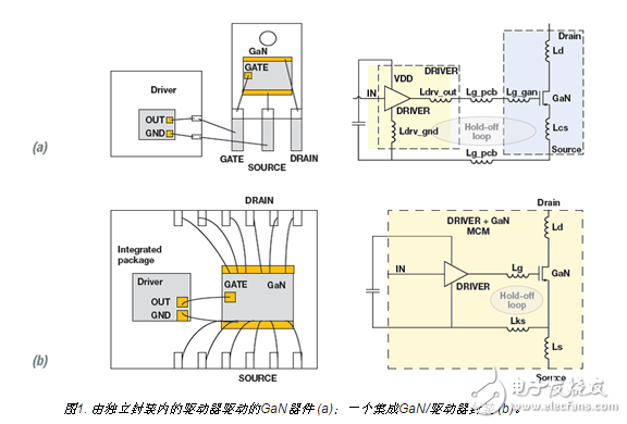
Figure 1. GaN device (a) driven by a driver in a separate package; an integrated GaN/drive package (b).
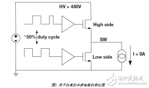
Figure 2. Simplified diagram of the half-bridge circuit used for simulation
Simulation settings
To simulate parasitic inductance effects, we used a depleted GaN half-bridge power stage with a direct drive configuration (Figure 2). We set the half bridge as a buck converter with a bus voltage of 480V, 50% duty cycle (output voltage [VOUT] = 240V) at 50ns dead time, and an 8A inductor current. This GaN gate is driven directly between the switching voltage levels. A resistive drive sets the turn-on slew rate of the GaN device. A current source only simulates an inductive load connected to a switch (SW) node in a continuous conduction mode buck converter.
Common source inductance
One of the most important parasitic elements in high-speed switching is the common source inductance (Lcs in Figure 1a), which limits the slew rate of the current drawn by the device. In a conventional TO-220 package, the GaN source flows from the bond wire to the leads, and both the draw current and the gate current flow therethrough. This common source inductor modulates the gate-to-source voltage as the current draws. The common source inductance is higher than 10nH (which includes wire bonds and package leads), which limits the slew rate (di/dt) and increases switching losses.
With the integrated package shown in Figure 1b, the driver ground is soldered directly to the source pads of the GaN die. This Kelvin source connection minimizes the common source inductance path shared by the power supply loop and the gate loop, allowing the device to switch at much higher current slew rates. A Kelvin source pin can be added to a discrete package; however, this extra pin makes it a non-standard power package. The Kelvin source pin must also be routed back from the printed circuit board (PCB) to the driver package, increasing the gate loop inductance.
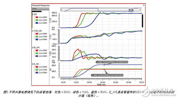
Figure 3. High tube turn-on with different common source inductances: red = 0nH, green = 1nH, blue = 5nH. E_HS is the integral value (energy consumption) of the VDS and IDS of the executive device during runtime.
Figure 3 shows the hard-switching waveform when the high-level switch is turned on. When the common source inductance is 5nH, the slew rate is halved due to the source degradation effect. A lower slew rate results in longer switching times, resulting in higher cross conduction losses, as shown in the energy consumption graph. When the common source inductance is 5nH, the energy loss increases from 53μJ to 85μJ, an increase of 60%. Assuming a switching frequency of 100 kHz, the power loss will increase from 5.3 W to 8.5 W.
Gate loop inductance
The gate loop inductance includes the gate inductance and the driver ground inductance. The gate inductance is the inductance between the driver output and the GaN gate. When using a separate package, the gate inductance includes a driver output bond wire (Ldrv_out), a GaN gate bond wire (Lg_gan), and a PCB trace (Lg_pcb), as shown in Figure 1a.
Depending on the package size, the gate inductance can range from a few nano hens in a compact surface mount package (eg, quad flat no-lead package) to more than 10nH in a leaded power package (eg, TO-220). If the driver is integrated into the same leadframe as the GaN FET (Figure 1b), the GaN gate is soldered directly to the driver output, which reduces the gate inductance to less than 1nH. Package integration can also greatly reduce driver ground inductance (from Ldrv_gnd + Ls_pcb in Figure 1a to Lks in Figure 1b).
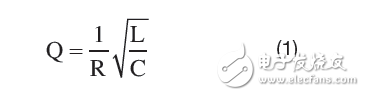
Reducing the gate loop inductance has a huge impact on switching performance, especially during turn-off, where the GaN gate is pulled down by a resistor. The resistor value of this resistor needs to be low enough so that the device does not turn back on during the switching due to the drain being pulled high. This resistor forms an inductor-resistor-capacitor (LRC) tank with the gate-source capacitance and gate-loop inductance of the GaN device. The Q quality factor in Equation 1 is expressed as:
Durable PITAKA MagCase For iPhone 6Plus Or 6S Plus make from 100% Aramid Fiber,which it was the same material used in body armor, spacecraft, jet engines, and Formula 1 Race cars.To profect your iPhone at safety condition in daily life.
Description:
1. 100% Brand new high quality Aramid Fiber, extremely durable!
2. Precision molded cases to perfectly fit your phone3. Resist dirt, stains and is anti-static and anti-slip
4. Washable material for easy cleaning
5. Protect your phone when in bumping.
6. Direct access to all ports and buttons without removing it from the case.
Color:black/silver/pink/blue/green/red/gold/purple etc
MagCase For iPhone 6Plus Or 6S Plus
iPhone 6Plus PITAKA Magcase,iPhone 6Plus PITAKA Magcase Aramid Fiber,iPhone 6Plus Phone Case,iPhone6S Plus Magcase 100% Aramid Fiber,iPhone6S Plus Magcase,Durable iPhone6S Plus Magcase
Shenzhen Aokal Technology Co., Ltd. , https://www.aokals.com