Since the high-power LED has a number of times higher than the low-power LED, the temperature rise will cause the flash rate to drop sharply. The specific internal substantive significance is to reduce the thermal impedance of the chip to the package, to limit the thermal impedance of the package to the Printed Circuit Board, and to improve the smooth and smooth heat dissipation of the chip. The most important thing is to find ways to reduce the thermal impedance and improve heat dissipation.
Click to download: Detailed explanation of several ways to improve LED heat dissipation performance
Cheap 12 Layers PCB stackup and thickness
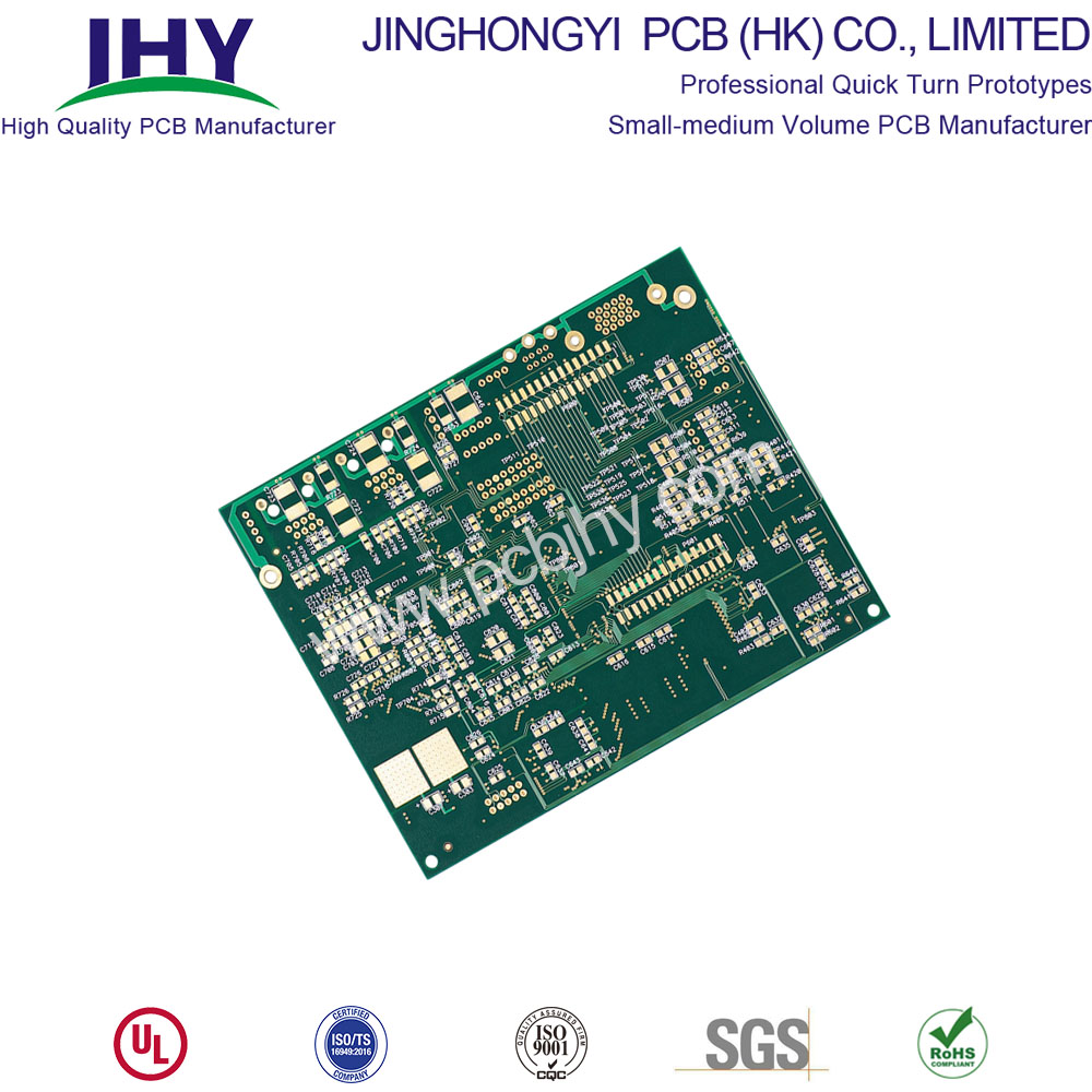
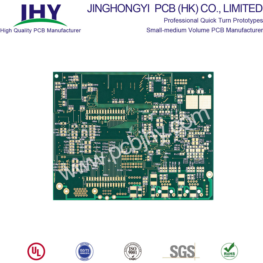
We are one of the few manufacturers in China that can manufacture 12-layer PCB boards on a large scale.
The 12-layer board can usually be manufactured smoothly on a 1.6mm thick FR-4 board. But we've seen more 14- to 16-layer boards are being fabricated into 1.6mm thick boards, but the number of manufacturers that can produce them is limited to manufacturers that can produce HDI boards. Those who can produce HDI boards are increasing.
12 Layers PCB– Heavy industry boards or boards with may tracks
For industrial PC design, 12-layer circuit boards are more popular. Compared with other multi-layer circuit boards, such as four-layer circuit boards, 8-layer circuit boards, 10-layer circuit boards, The price of the 12-layer PCB is still reasonable.

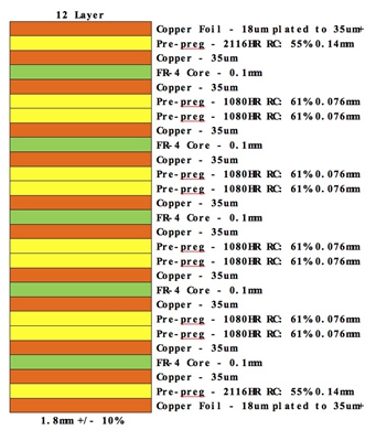
12 Layer PCB stackup and thickness
12 Layer PCB Stack Up
Top Layer †18um Copper Foil (plated to 35um+)
Preâ€Preg †1 x 2116
Layer 2 & 3 †0.13mm Frâ€4 Core with 35um/35um Copper
Preâ€Preg †1 x 2116
Layer 4 & 5 †0.13mm Frâ€4 Core with 35um/35um Copper
Preâ€Preg †1 x 2116
Layer 6 & 7 †0.13mm Frâ€4 Core with 35um/35um Copper
Preâ€Preg †1 x 2116
Layer 8 & 9 †0.13mm Frâ€4 Core with 35um/35um Copper
Preâ€Preg †1 x 2116
Layer 10 & 11 †0.13mm Frâ€4 Core with 35um/35um Copper
Preâ€Preg †1 x 2116
Bottom Layer †18um Copper Foil (plated to 35um+)
Stardand 12 Layer PCB 1.6mm +/†10%

12 layer stackup – 4 GNDs
I use this stackup a lot, provides GND shielding of high speed signals and has tightly coupled Power-Ground planes:
Signal / Solid GND plane / High speed signals and important buses / Solid GND plane / Power / Power or Mixed with signals / Power or Mixed with signals / Power / Solid GND plane / High speed signals and important buses / Solid GND plane / Signal
12 layer stackup – two additional signal layers
Signal / Solid GND plane / Signal / Signal / Solid Power Plane / Power or Mixed with signals / Power or Mixed with signals / Solid Power Plane / Signal / Signal / Solid GND plane / Signal
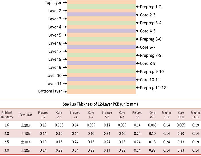
12 layer PCB stackup thickness


12 layer PCB Features and benefits
- Lead-free surface finish and lead-free components
- Long storage time (vacuum and anti-static packaging)
- Improved the speed of signal transmission
- Fast on time delivery
- UL certified and RoHS compliant
- Prototype PCB Manufacturing
12 layer PCB Application
DSL Modem, Solar Battery Charger, Vehicle Tracker, GPS Receiver, Wi Fi Antenna, Bluetooth USB Hub, USB Wireless Router, SMS Modem, Multicoupler Antenna, Phone systems.
12 Layer PCB
Printed Wiring Board,Custom Printed Circuit Board,12 Layer PCB,Custom 12 Layer PCB
JingHongYi PCB (HK) Co., Limited , http://www.pcbjhy.com
