
Cable and satellite content providers are constantly introducing new services to fiercely competitive markets. These new services include Internet access, video on demand, support for DVD/CD players and hard drives, which are enabling a simple set-top box (STB) to evolve into a powerful home gateway. These advanced set-top boxes form a local area network (LAN) at home. Therefore, the set-top box generally has an Ethernet or Firewire port, or other communication methods, and may even be Bluetooth. These more complex set-top boxes in turn require more power. As these systems consume more power, system designers are increasingly concerned about issues such as temperature rise, time to market, efficiency, regulatory approval, cost, power sequencing, and power factor correction (PFC).
This article refers to the address: http://
One way to address these concerns is to change the power architecture from a traditional multi-output flyback power supply to a higher performance, more flexible distributed power architecture with point-of-load (POL) regulators. Most set-top boxes currently use an off-line, multi-output flyback power architecture. These power supplies provide 30W of power with up to 65% conversion efficiency. The advanced set-top box power supply delivers up to 65W with a single distributed DC voltage (eg 12V) and a downstream point-of-load regulator with an overall conversion efficiency of up to 80%.
The services provided by the content provider determine the characteristics of the set-top box, such as processor power consumption, modem speed, transmission media, whether it includes a DVD player or hard drive, and the number of I/O ports. The standard architecture for set-top boxes is based on the External Device Computer Interface (PCI) bus, which looks like a notebook PC from the surface. However, although the PC architecture is the same all over the world, the set-top box architecture in different regions and even different manufacturers has changed a lot. Of course, because the needs of consumers are easy to change, as the service changes, the set-top box configuration is constantly changing. The function determines the power requirements, and the only obvious trend is that the system power consumption is increasing. Competition and regional differences between service providers mean that there is considerable pressure to get set-top boxes on time. Delayed delivery due to power supply design is intolerable as this may lose market share.
It is common for set-top box power supplies to change later in the design cycle. However, the least desirable thing is to delay the development of the set-top box due to the power supply, but this can happen if an offline multi-output flyback power supply is required. It can take 6 to 9 months, or even up to a year, to design such a power supply and get regulatory approval for safety and EMI performance. With a multi-output flyback design, late changes can result in the need to repeatedly design magnetic components over time. Therefore, in some cases, desperate designers will increase the diode drop to accommodate the last change in output voltage or current demand.
The standard off-the-shelf AC input (90V to 26?V AC) single output power supply has the advantage of being approved by the safety department and the EMI regulatory authority. These power supplies achieve up to 90% power conversion efficiency with a single output voltage of 3.3V to 48V. In addition, the standard single-sale output power supply is not expensive, available in several sizes, mass production, suitable for many applications. Using this power supply can shorten the development cycle by 6 months. Even if the maximum power is increased, it doesn't matter, because considering the possibility of higher power, designers can plan for 20% to 30% redundancy from the beginning, which does not increase the cost or occupy a lot of board space.
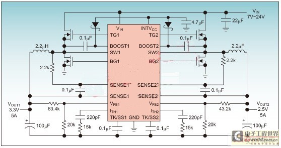
Figure 1: Schematic diagram of a dual 3.3V/2.5V output LTC3850 operating from a 7V to 24V supply.
Power factor correction is another problem that affects the power of the set top box. The IEC/EN61000-3-2 specification limits the harmonic current radiation for power supply systems with input powers greater than or equal to 75W. In fact, this specification requires additional circuitry when the input power exceeds 75W. A multi-output, flyback power supply with 65% efficiency provides 49W of maximum output power when no additional power factor correction circuitry is required. A distributed power supply with 90% efficiency combined with a downstream point-of-load regulator with 90% to 95% efficiency provides 60W to 6?W power without a power factor correction circuit. The obvious benefits of higher efficiency are reduced heat, reduced ventilation requirements, and extended mean time between failure (MTBF) times.
Linear Technology offers a complete line of high efficiency synchronous point-of-load DC/DC switching regulators including modules, monolithic circuits and controllers. The LTC3850 is a recently introduced dual output point-of-load DC/DC switching regulator controller that converts 12V to 5V/5A with 95% efficiency or converts 12V to 3.3V/5A with 92% efficiency and 91 The efficiency of % converts 12V to 2.5V/5A.
The LTC3850 is a dual output synchronous step-down switching regulator controller that drives all N-channel power MOSFET stage circuits. Its 4V to 24V input range is suitable for a wide range of applications, including most intermediate bus voltage applications. Powerful on-chip drivers allow the use of high-power external N-channel MOSFETs that can output voltages from 0.8V to 5.5V while delivering up to 20A of output current.
Dual Output, 5A Regulator with DCR Detection
Figure 1 shows an LTC3850-based circuit that operates from a 7V to 24V input range with a switching frequency of 530kHz and eliminates the need for a current sense resistor, providing independent outputs of 2.5V/5A and 3.3V/5A. By using the DC resistance of the inductor as a current sensing unit, the application circuit consumes the lowest possible power at full load current. The efficiency is higher than 90%, and the efficiency curve is shown in Figure 2.

Figure 2: Efficiency curve of the circuit of Figure 1.
Tracking benefits
Tracking provides a predictable way to adjust the output power up or down. The feedback voltage is typically kept below the internal reference voltage or the voltage on the TRACK pin during tracking. Further, the LTC3850 combines the tracking and soft-start functions (TK/SS pins) of each channel in one pin and customizes the switching mode of operation according to the state of the TK/SS pin. Figure 3 shows the consistency tracking and proportional tracking curves, which can be configured with the LTC3850.

Figure 3: Two different output voltage tracking modes implemented with the LTC3850.
Fast transient response
The stability of any regulator feedback loop can be checked by looking at the load current transient response. Switching regulators require several cycles to respond to sudden changes in output load current or changes in input voltage. When a step load occurs, the amount of change in VOUT is equal to ?ILOAD multiplied by the ESR of the output capacitor, where ESR is the equivalent series resistance. ILOAD also begins to charge or discharge COUT, generating a feedback error signal that forces the regulator to adapt to current changes and return VOUT to a steady state value. During this recovery process, you can monitor VOUT for excessive overshoot or ringing to indicate if there is a stability issue. Figure 4 shows the transient response of the LTC3850 circuit in Figure 1. The recovery process is well attenuated, with a 50% settling time less than 50us. The maximum deviation of the output voltage from the nominal value can be reduced by increasing the output capacitance.

Figure 4: LTC3850 transient response for the circuit of Figure 3.
Light load work
The LTC3850 operates in constant frequency PWM mode during heavy loads. At light loads, it can be switched between three modes: continuous, pulse skip or burst mode. Burst mode operation switches between bursts of one cycle to several cycles, and the output capacitor provides energy during the sleep interval. This allows for the highest possible light load efficiency. The forced continuous mode is always in PWM mode from no load to full load, achieving the lowest possible output voltage ripple. The pulse skip mode operates at a constant frequency, but always turns off the synchronous switch before allowing the inductor current to reverse. This approach reduces ripple at light loads compared to burst mode operation, while improving efficiency at light loads compared to forced continuous mode.
Each channel also has a separate RUN pin with an accurate 1.2V turn-on threshold. When the LTC3850's own current source is used to charge the soft-start capacitor, the RUN pin of one channel goes high and the soft-start capacitor begins to charge within approximately 80us. As an alternative, any RUN pin can be held high while TK/SS is low, keeping the internal 5V regulator as a standby supply. This feature can be used to power the wake-up circuit, while the wake-up circuit controls the state of the two TK/SS pins.
Fixed operating frequency / minimum on time
The LTC3850's two channels operate in different phases, thus reducing input RMS current ripple and reducing input capacitance requirements. The switching frequency can be adjusted from 250kHz to 780kHz, either with the voltage setting on the FREQ/PLLFLTR pin or with a phase-locked loop to the external clock input to the MODE/PLLIN pin. At high frequencies, the LTC3850 can operate normally with a low duty cycle due to its short on-time switch. For example, a 15V to 1.1V converter operating at 700kHz requires a minimum turn-on time of less than
1.1V_ __ = 104ns
(15V)? (700kHz)
The LTC3850 can make this powerful low-duty-cycle application a reality by operating its powerful top-gate driver for a period of only 90ns.
Two methods of detecting current
The LTC3850 has a complete differential comparator that can be used to sense the current through the inductor. The SENSE+ and SENSE- pins can be connected to a current sense resistor in series with the inductor or to an RC network in parallel with the output inductor to achieve high energy efficiency detection across the inductor DC resistance (DCR sense). DCR detection prevents power loss due to sense resistors, but with typical embedding errors of 5% to 10%, which is acceptable for most applications. The LTC3850 can be designed in either of two ways for design flexibility and has three pin-selectable current-limit thresholds.
When the output is shorted, the LTC3850 limits the peak current cycle by cycle to protect the input supply and power components. When the inductor peak current detection threshold of 130% of VSENSE(MAX)/RSENSE is reached, the main MOSFET is turned off. VSENSE(MAX) can be set to 30mV, 50mV or 75mV to achieve multiple output current values. The duty cycle has a very small effect on the current limit. In the case where the load current is higher than the maximum programmed value but lower than the hardware short-circuit current value, the LTC3850 can smoothly shorten the turn-on time of the top MOSFET and lower the output voltage. The LTC3850 also protects itself from undervoltage input and overvoltage output voltage damage. The RUN pin can be referenced to a voltage divider on the VIN pin to control the output state with their precise thresholds. If the output voltage is 7.5% higher than the target value, the bottom MOSFET can remain on until the regulation is restored. If the LTC3850 is allowed to operate at an input voltage close to the output voltage programmed value, its duty cycle can be as high as 97%.
The LTC3850 is available in a small 4mm x 4mm QFN-28 (0.4mm pitch), 4mm x 5mm QFN-28 (0.5mm pitch) or 28-pin narrow SSOP package. The device operates at high efficiency with or without DCR current sensing. Tracking, very fast response times, powerful on-chip MOSFET gate drivers, two-phase operation, external synchronization, and low cost allow the LTC3850 to be used in set-top boxes and many other applications.
Summary of this article
The load point adjustment is more efficient than the traditional multi-output offline custom flyback power supply, which can improve the performance of the set-top box design. Point-of-load regulation enables higher output power without the need for additional power factor correction circuitry, and speeds time-to-market by using regulatory-supplied, single-supply output power supplies and high-efficiency point-of-load downstream regulators. The LTC3850's feature-rich, high-efficiency, and small package size provides an ideal solution for set-top box power supply designers.
Neon Sign Design,Directional Neon Signs,Trendy Neon Signs,Awesome Neon Signs
Shenzhen Oleda Technology Co.,Ltd , http://www.baiyangsign.com