
As high power LEDs are increasingly used in general lighting, there is an increasing demand for off-line power supplies that drive these LEDs. Due to the VI (voltage-current) characteristics of the LED, the output current of this Power Supply must be constant current. This article will discuss a power supply based on a Fast Power Switch (FPS) that achieves a secondary constant current output through primary side regulation. Because the power supply eliminates the need for op amps and optocouplers to stabilize the output current, it is cost effective when safety isolation is required.
Traditional constant current output PSU
Figure 1 shows a conventional constant current output off-line power supply based on a flyback topology that provides 700mA and 5.1V maximum output voltage from 85 VRMS to 265 VRMS. According to its technical data, the power supply should be able to drive 3W high power LEDs. This circuit is simple and easy to understand: the mains input rectification (BD1 - BD4) and filtering (C2, C3 and L1), followed by a flyback circuit with FPS FSQ510.
The FSQ510 is a "minimum" member of the integrated circuit family that implements all of the features of advanced switching power supplies, and is a single-chip device that integrates 700V Sense-FETs, while those with higher power are dual-chip devices. Includes a controller and a separate Sense-FET with VDS=650V. Since the basic functions and behaviors of all members of this series are almost identical, the discussion of power supplies using the FSQ510 can be applied to the entire series. By connecting the power supply to the mains, the internal startup circuit of the device can be started, that is, the internal high-voltage JFET charges C8 to a typical 13V startup voltage. Once this level is reached, the internal Power-MOSFET enters the switch operation and the power supply begins to operate normally. At this point, the JFET is turned off to reduce power consumption; while the FPSTM is powered by a separate transformer winding, D2 rectified, and R7 and C8 filtered.
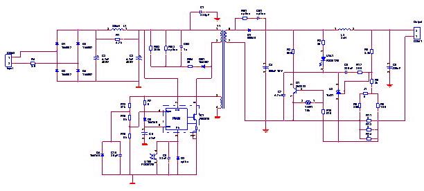
Figure 1: Traditional constant current output power supply
RS2 and RS3 and DS1 and C82 form a clamp circuit (commonly known as a "buffer") network that absorbs the energy stored in the leakage inductance of the transformer. This is to limit the drain voltage to a safe level.
The secondary voltage of the transformer is filtered by D1 and C4, and filtered by L2 and C5. The output voltage is regulated by a circuit consisting of R2, R3, R5, R6, U1, and U2. U1 couples the feedback signal to the primary, while C6 and R17 form the frequency compensation circuit, resulting in a stable dead loop.
The actual output current in this example is sensed by the shunt resistor R11|R13|R14 and is adjusted by means of Q1 and U1. When the voltage drop across the shunt resistor exceeds VBE of Q1, there will be current flowing through the U1 LED, which will reduce the voltage on the FPSTM feedback pin. In this way, the duty cycle of the Power-MOSFET is reduced, eventually reducing the output voltage and output current. Since the VBE of the bipolar transistor (BJT) is very temperature sensitive, a compensation circuit consisting of R10 and NTC THR1 is added. The role of R8 and R9 is to cut off U2, preventing the voltage loop from affecting the normal operation of the current regulation loop.
R12, R15, R16, D4, and C10 form the circuit that implements the quasi-resonant switching function of the power MOSFET in FPSTM. A quasi-resonant switch refers to monitoring the drain voltage, and the MOSFET is turned on only when the drain voltage is at a minimum. Here, a physical fact is taken that the drain voltage oscillation occurs when all the energy stored in the transformer is transferred to the secondary. This oscillation is caused by a resonant circuit formed by the magnetizing inductance of the transformer and the drain-source capacitance of the MOSFET. Since the switch is turned on at the minimum drain voltage, the switching loss is greatly reduced and the EMI performance is improved. This synchronous circuit is not actually connected directly to the drain of the MOSFET, but to the transformer winding VCC with the same waveform but lower voltage amplitude.
Primary regulated constant current power supply
In the flyback converter circuit, the output voltage can be well adjusted without special adjustment of the circuit. This is because (for example, parasitic effects are ignored) the ratio of the two output voltages is equal to the ratio of the turns of the respective transformer windings, so that it is possible to adjust, for example, the VCC winding voltage to obtain a fairly stable isolated output without the need for an optocoupler. Figure 2 shows a primary regulated power supply that still does not have constant current characteristics.
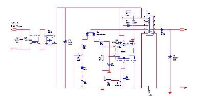
Figure 2: Power supply with primary regulation with constant output voltage
Most of the circuits for this type of power supply are the same as those with secondary regulation, but the feedback loop is completely different.
As mentioned earlier, the feedback comes from the same transformer winding that supplies the FPS. This voltage is rectified by D3, applied to R2/C7 that produces the chip VCC, and R4/C4 that filters the feedback voltage. In general, the feedback signal can also be taken from C7. However, since a relatively large capacitance is required to support the startup current consumption, it is preferable to use additional channels having different time constants. Zener diode D7 provides the base current for Q1 used as an error amplifier. If VCC and the output voltage rise at this time, the base current of the transistor will also increase, thereby lowering the level on the FPSTM feedback pin, similar to the power supply using the optocoupler feedback.
At this point, the power supply is still operating in constant voltage mode. How do you turn it into a current source? If you analyze the relationship between the output current of the flyback switch and the peak MOSFET current in continuous conduction mode, you know that to get a constant output current, the peak MOSFET current must be proportional to the output voltage VOut and inversely proportional to the input voltage VIn. . In discontinuous conduction mode, the leakage current must be proportional to the square root of VOut and theoretically independent of VIn.
The FPSTM power switch FSQ0170RNA used in the power supply has an input called 'ILim'. This input helps to construct the primary regulated current source and sets the maximum peak leakage current of the MOSFET. The method is to connect a resistor to this input pin or draw a certain current from this pin. If the resistor is connected to this pin, the peak leakage current will not exceed a certain set value.
The principle of the current source can be explained with the aid of FIG. It can be clearly seen from the figure that this constant voltage PSR power supply can be turned into a current source by simply adding some of the lowest cost passive components.
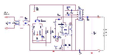
Figure 3: Constant current output power supply with primary regulation
In this circuit, the positive and negative voltages of the VCC winding are rectified by D5, and each is filtered by an R/C circuit (R3/C5 and R4/C4 filter circuits, respectively). The positive portion through C4 is proportional to the output voltage, while the negative portion through C5 is related to the input voltage of the power supply and negative to the ground on the primary side. As long as the load current is small, the regulation loop formed by D7, R8, R9 and Q1 works in the same way as in Figure 2. Unlike Figure 2, R8 is not connected to the primary ground, but is connected to the negative voltage of C5. As long as the power supply is operating in voltage mode, the voltage at the node including the D7 cathode is almost equal to the base voltage VBE of Q1, and only a small current flows from pin 4 through R7. When the load current increases, the peak current on the primary side will also increase. When the maximum peak current on the primary side, which is mainly determined by R7, is reached, the output voltage begins to decrease, which also causes the voltage of the D7 cathode to drop; and the current flowing through R7 will This will increase, which is the result of a further drop in the peak current of the MOSFET. With proper R7 selection, this peak current is proportional to the output voltage and the output current is almost constant. R6 is used to compensate for changes in the output current as the input voltage increases. In constant current mode, Q1 is in a negative bias state and is therefore fully turned off. In a constant voltage supply, this means that a fault has occurred and the voltage on the VFB pin will rise to 6V and the device will shut down. To prevent this from happening, R10 is added to the circuit.
Since the output voltage of the current source varies significantly with the load, the voltage of the VCC winding also changes significantly. Therefore, the winding turns ratio must be properly chosen so that the chip supply voltage is above the undervoltage lockout level of the FPSTM at the minimum output voltage. Since the VCC voltage range may be wide, the Zener diode D6 must be added to prevent the chip from entering an overvoltage shutdown state.
The LED ballast circuit diagram shown in Figure 3 is capable of outputting 700 mA nominal current to drive 3 to 5 high power LEDs with European mains input. Figure 4 shows the output characteristics. At very small load currents, the voltage rises very high, which is common in PSR power supplies. The voltage is fairly constant in the medium to high current range. This section is not the focus of LED ballasts. The point is that the load current remains constant over a wide output voltage range in constant current mode.
Figure 4: VI characteristics of the power supply shown in Figure 3.
Fast Semiconductor offers a variety of versions, such as 350mA output current or global commons input circuit, transformer specifications and PCB data.
(Author: Michael Weirich)
Capacitor Switch,Vacuum Switch,Transformer Switch
Vacuum Circuit Breaker Co., Ltd. , http://www.nstransformer.com