
The field terminal in the distributed control system is generally composed of a controller and each detection module, and a data exchange link is established between them through a certain communication network. This system has the advantages of high reliability, openness, flexibility, coordination, and easy maintenance. However, the distributed system also has the characteristics of a large number of terminals and a wide distribution range. Once the terminal system software is defective or the user proposes new functions and indicators, the workload and cost of upgrading and maintenance are very large. In view of the above situation, this paper designs a convenient, flexible, fast and stable mechanism for online update of MCU nodes. Based on the CAN network composed of LPC11C24 microcontroller, IAP programming technology (In ApplicaTIon Programming) is used to realize the software update function to the target node MCU.
NXP Semiconductors (NXP) introduces the industry's first embedded easy-to-use on-chip CANopen driver, integrated high-speed CAN physical layer transceiver microcontrollers LPC11C22 and LPC11C24. As a unique system-level packaging solution, LPC11C22 and LPC11C24 are integrated The TJF1051CAN transceiver implements full CAN functionality in a low-cost LQFP48 package.
The Controller Area Network (CAN) was developed by the German company BOSCH, which is known for its research and development and production of automotive electronics, and eventually became an international standard (ISO11898). It is one of the most widely used fieldbuses in the world. In recent years, its high reliability and good error detection capability have been valued and widely used in automotive computer control systems and industrial environments with harsh ambient temperatures, strong electromagnetic radiation and high vibration.
The system architecture is mainly composed of two parts: a CAN network composed of various MCUs; a USB-CAN communication card installed on a PC can connect the PC to the CAN network for data communication. The system architecture is shown in Figure 1. The software also includes two parts: the upper computer software running on the PC, providing the user operation interface, sending the application code to the node through the CAN bus; the startup program running on the node mainly responds to the download command, accepts the code, writes the code Into the FLASH, boot the application.

Figure 1 System Architecture
3.1 IAP programming technology
IAP is a programming mode applied in the FLASH program memory, that is, the FLASH read/write operation is completed under the control of a certain program, and the read and write operations on a certain segment, a certain page, or even a certain byte can be controlled.
The LPC11C24 microcontroller supports and provides 9 IAP commands:
1 sector to prepare for writing;
2 copy the RAM content to FLASH;
3 erase the sector;
4 sectors check empty;
5 read device ID;
6 read the boot code version;
7 comparison;
8 recall the ISP;
9 read UID.
LPC11C24 has 32KB of FLASH space, which is divided into 8 sectors, each sector has a size of 4KB. In order to make the program update and application more independent, this paper divides the FLASH space into three areas, which are the startup program area. Application area, user data area.
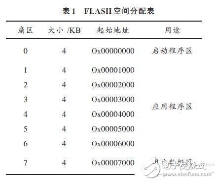
The 1 startup program is a specific resident code, which is specially used to receive new code from the host, and burn it to the corresponding FLASH space. After completion, it jumps to the application code area to execute the new program, and the code is relatively small. The compiled image file is less than 4KB, and the startup program is executed each time the system is powered on or restarted.
2 Applications are code that truly implements user functions.
The 3 user data area is some settings and data used to store the application.
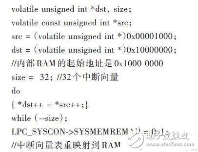
LPC11C24 supports 32 vector interrupts. The interrupt vector table is located in the first 4KB space of FLASH by default. The address is from 0x00000000~0x00000079. According to the previous design, the startup program occupies the first 4KB space. When jumping to the application, the actual The interrupt vector table is located in the space of 0x00001000~0x00001079. However, the LPC11C24 series of microcontrollers do not support the address of the custom interrupt vector table. It only supports re-mapping the interrupt vector table from FLASH to RAM.
In order for the application to implement normal interrupt handling, the startup program needs to copy and map the application's interrupt vector table to RAM before jumping to the application [10].
The code example is as follows:
The programs are written and compiled in the Keil for ARM integrated environment.
First, create a new LPC11C24-based project under Keil software, and configure the starting address and size of FLASH and SRMA. The details are shown in Table 2.

Define the address of the application in the startup program, #defineAPP_CODE_ADDR (0x00001000), the code of the program jump is written in assembly language, the code example is as follows:

Windshield Cell Phone Mount,Car Windscreen Mobile Phone Holder,Car Windshield Cell Phone Holder,Car Windscreen Cell Phone Holder
Ningbo Luke Automotive Supplies Ltd. , https://www.nbluke.com