
1 Introduction
In recent years, data collection and its application have received more and more attention, and data acquisition systems have also developed rapidly. It can be widely used in various fields.
Data acquisition technology is one of the important branches of information science. Data acquisition is also the process of obtaining object information from one or more signals. Data acquisition is an important part of industrial control systems. It is usually implemented by some relatively independent single-chip microcomputer systems. As an indispensable part of the measurement and control system, the performance characteristics of data acquisition directly affect the whole system.
Voltage measurement is the most common, and methods and instruments for designing and improving voltage measurement accuracy are of great significance. In the voltage measurement design, the microcontroller is the core of the entire design. In addition to this, there must be an analog-to-digital converter (ADC) in the design. The ADC is used to directly capture the analog voltage and convert the analog signal into a digital signal, which directly affects the accuracy and speed of data acquisition.
2. System Overview
The microcontroller of this design uses STM32 microcontroller.
The STM32 family of microcontrollers is based on the ARM Cortex-M3 core. With a clock frequency of 72MHz, it is a high-performance product in its class. It has the advantages of high performance, low cost and low power consumption. It is a good choice for embedded application design. The A/D converter in the design uses the STM32 built-in ADC. The STM32 ADC is a 12-bit successive approximation analog-to-digital converter.
It has up to 18 channels and can measure 16 external and 2 internal sources. The A/D conversion of each channel can be performed in a single, continuous, scan or discontinuous mode. The conversion result can be stored in a 16-bit data register in left or right alignment. Its input clock can reach up to 14MHz.
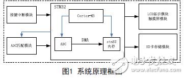
This design can measure the voltage of 8 channels, the measuring range is 0-10V, the display error is ±0.001V. LCD displays the voltage value and waveform diagram in real time, and the MicroSD card stores the data synchronously. The system block diagram is shown in Figure 1.
3. System hardware design
The hardware of this design mainly includes STM32 module, LCD module, SD card module and button module. The STM32 module not only acts as a core controller, but also includes ADC devices, which mainly include the STM32 minimum system circuit. The LCD module mainly includes an LCD drive interface circuit. The SD card module is mainly an SD card driver circuit. In addition to this, there are J-Link interface circuits and power supply circuits for program download and debugging.
3.1 STM32 minimum system
This module mainly introduces the peripheral modules used in the STM32 chip and design.
The STM32 minimum system uses an external high-speed clock with an external 8M crystal. The two BOOT pins of the STM32 are tied low to allow the user flash memory to be the program boot area. The chip uses the J-L ink download mode and can also be used for hardware debugging. The power supply pins of the STM32 are connected with filter capacitors to ensure the stability of the microcontroller power supply.
The STM32F103VET6 has three ADCs that can be used independently or in dual mode (increasing the sample rate). The STM32's ADC is a 12-bit successive approximation analog-to-digital converter. It has 18 channels to measure 16 external and 2 internal sources. The A/D conversion of each channel can be performed in a single, continuous, scan or discontinuous mode. The results of the ADC can be stored in a 16-bit data register in left or right alignment. The maximum conversion rate of the STM32 ADC is 1Mhz, that is, the conversion time is 1us (ADCCLK=14M, the sampling period is 1.5 ADC clocks), and the ADC clock cannot exceed 14M, otherwise the accuracy of the result will decrease. The STM32 divides the conversion of the ADC into two channel groups: a regular channel group and an injection channel group. A regular channel is equivalent to a running program, and an injection channel is equivalent to an interrupt. When the program is executed normally, the interrupt can interrupt the normal execution of the program. Similar to this, the conversion of the injection channel can interrupt the conversion of the regular channel, and the regular channel can continue to be converted after the injection channel is converted.
The data collected by the ADC in this design is transmitted using DMA to achieve high-speed real-time purposes.
3.2 ADC control circuit
The STM32's digital/analog conversion module (DAC) is a 12-bit digital input, voltage output digital/analog converter. The DAC is used in this design to control the gain of the ADC matching circuit.
On the basis of turning on the DAC module power supply and configuring the GPIO required by the DAC, write data to the data DAC_DHRx register of the DAC channel. If the hardware trigger is not selected, the data stored in the register DAC_DHRx will be automatically transferred to the register after one APB1 clock cycle. DAC_DORx. Once data is loaded from the DAC_DHRx register into the DAC_DORx register, the output is asserted after a certain amount of time. The length of this period varies depending on the supply voltage and the analog output load.
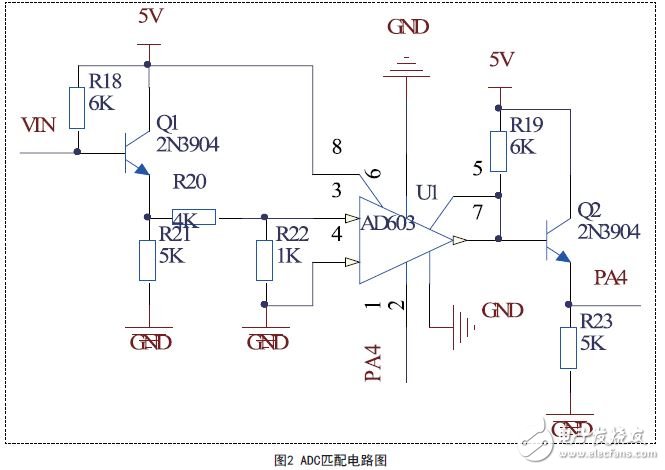
In order to expand the measurement range and measurement accuracy, this design adds a matching circuit to the STM32's ADC. In the ADC control circuit, the input signal passes through the emitter voltage follower circuit and then passes through the voltage divider circuit to make the input signal meet the input requirements of AD603. It is then passed through the emitter voltage follower circuit and input to the ADC input. The control input of the AD603 uses the STM32 DAC to meet the gain requirements.
The matching circuit is centered on AD603. The AD603 is a single channel, low noise, linearly continuously adjustable gain amplifier with variable gain range. When the bandwidth is 90MHz, the gain varies from -10dB to +30dB; when the bandwidth is 9M, the range is 10~50dB.
Short-circuit VOUT and FDBK, that is, broadband mode (90MHz wideband), the gain of AD603 is set to -11.07dB~+31.07dB. The 5rd and 7th pins of AD603 are connected, and the adjustable range of single AD603 is -10dB~30dB. The gain of the AD603 is linear with the control voltage. The gain control terminal has an input voltage range of ±500mv and a gain adjustment range of 40dB. When the step is 5dB, the control terminal voltage needs to be increased:
![]()
The circuit diagram of the ADC matching circuit is shown in Figure 2.
3.3 LCD control circuit
The LCD used in this design is 2.4 inches, 320 & TImes; 240 resolution. The LCD module is controlled using the FSMC interface of the STM32.
The FSMC (Flexible StaTIc Memory Controller) can be a static storage controller. It is a storage control mechanism unique to the STM32 series that integrates more than 256KB of Flash and suffixes xC, xD and xE. By setting special function registers, FSMC can issue corresponding data/address/control signal types to match the speed of signals according to different external memory types, so that STM32 series microcontrollers can not only apply different types and speeds. External static memory, and can expand a variety of different types of static memory without adding external devices, to meet the comprehensive requirements of system design for storage capacity, product size and cost.
Inside the STM32, one end of the FSMC is connected to the core Cortex-M3 via the internal high-speed bus AHB and the external bus is oriented to the extended memory. After the core sends an access signal to the external memory to the AHB bus, it is converted into a signal conforming to the external memory communication protocol by the FSMC, and sent to the corresponding pin of the external memory to implement data interaction between the core and the external memory. The FSMC acts as a bridge, enabling both signal type conversion and signal width and timing adjustment to mask differences in different memory types, making it no different for the core.
The FSMC can be connected to devices such as NOR/PSRAM/NAND/PC cards, and has 26 address buses of FSMC_A[25:0], and 16 data buses of FSMC[15:0]. In addition, the storage space of the FSMC extension is divided into 8 blocks. The block of operation is selected by the address line. Thus, the LCD will be treated as a memory with an address space.
Ultrasonic Annunciator,Ultrasonic Piezo Annunciator,Outdoor Ultrasonic Annunciator,Ultrasonic Piezoelectric Annunciator
NINGBO SANCO ELECTRONICS CO., LTD. , https://www.sancobuzzer.com