
The development of cellular communications is increasingly tied to advanced modulation schemes. In the latest generation (2.5G and 3G) base stations, the design strategy includes methods to achieve high linearity while minimizing power consumption. For example, by monitoring the performance of a base station power amplifier (PA), the output power of the PA can be maximized while obtaining the best linearity and efficiency. Fortunately, with discrete integrated circuits (ICs) tailored for this purpose, the output level of the PA can be easily monitored.
The performance of wireless base stations in terms of power consumption, linearity, efficiency and cost mainly depends on the PA in the signal chain. The low-cost and high-power performance advantages of silicon laterally diffused metal oxide semiconductor (LDMOS) transistors are very suitable for modern cellular base station PA design. The inherent balance of linearity, efficiency, and gain determines the optimal bias conditions for LDMOS PA transistors.
For environmental reasons, the optimization of base station power efficiency is also an important consideration for companies in the telecommunications industry. In order to reduce the total energy consumption of base stations to reduce their impact on the environment, the industry is making unremitting efforts. The daily operation cost of the base station mainly comes from the consumption of electric energy, among which, the electric energy consumed by the PA may account for more than half. Therefore, optimizing the power efficiency of the PA can improve the operating performance of the base station, help to protect the environment and improve economic efficiency.
Controlling the drain bias current to keep it constant during temperature and time changes can significantly improve the overall performance of the PA while ensuring that its output power level remains within the specified range. One method of controlling the gate bias current is to optimize the gate voltage by fixing the gate voltage with a resistive voltage divider during the test / evaluation phase.
Although this fixed gate voltage solution is quite cost-effective, it has one major drawback, which is that it does not take into account environmental changes, manufacturing extensibility, or power supply voltage changes. Using a high-resolution digital-to-analog converter (DAC) or a lower-resolution digital potentiometer to dynamically control the PA gate voltage can provide better control of the output power. With user-programmable gate voltage, the PA can maintain optimal bias conditions even if voltage, temperature, and other environmental parameters change.
The two main factors affecting the PA drain bias current are the high-voltage power supply line change of the PA and the on-chip temperature change. The drain voltage of the PA transistor is easily affected by changes in the high-voltage power supply line. By using a high-side current (I) detection amplifier to accurately measure the current on the high-voltage power supply line, the drain voltage of the PA transistor can be monitored. The full-scale current reading is set by an external sense resistor (R). In applications monitoring extremely high currents, this sense resistor must be able to dissipate I2R losses. If the rated power consumption of the resistor is exceeded, the resistance value may shift or the resistor may fail completely, which will cause the differential voltage across the resistor to exceed the absolute maximum rating.
The measured voltage represented by the current sensor output can be multiplexed into the analog-to-digital converter (ADC) to generate the digital data required for monitoring. Care should be taken to ensure that the output voltage of the current sensor should be as close as possible to the full-scale analog input range of the ADC. Through continuous monitoring of the high-voltage line, when a surge voltage is detected on the power supply line, the power amplifier can readjust its gate voltage to maintain the optimal bias conditions.
The drain-source current IDS of the LDMOS transistor has two temperature-related items, namely the effective electron mobility μ and the threshold voltage Vth:
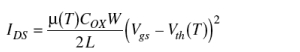
The threshold voltage and effective electron mobility decrease with increasing temperature. Therefore, changes in temperature will cause changes in output power. Using one or more discrete temperature sensors to measure the temperature of the PA, you can monitor the temperature changes on the circuit board. There are a variety of discrete temperature sensors that can meet system requirements, from a variety of analog voltage output temperature sensors to various digital output temperature sensors with single wire, I2C bus and serial peripheral interface (SPI) control.
The output voltage of the temperature sensor is multiplexed into the ADC, so that the temperature data is converted into digital data for monitoring (Figure 1). Depending on the system configuration, multiple temperature sensors may be required on the circuit board. For example, if more than one PA is used or multiple front-end drivers are required, using a temperature sensor for each amplifier can better control the system. In this case, a multi-channel ADC is required to convert the analog output of the temperature sensor. At present, all kinds of ADCs generally have a built-in over-range alarm function, and a warning will be issued when the input exceeds the set limit. In the PA signal chain, this function is of great significance for monitoring temperature and current sensor readings. Both the upper and lower limits can be set in advance, and only when these limits are exceeded will a warning signal be issued.
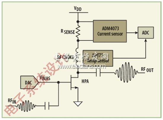
Figure 1: This block diagram shows a simplified control system using an ADT75 temperature sensor and ADM4073 current sensor multiplexed into the ADC model.
Innosilicon is a worldwide one-stop provider of high-speed mixed signal IPs and ASIC customization with leading market shares in Asian-Pacific market for 10 consecutive years. Its IP has enabled billions of SoC's to enter mass production, covering nodes from 180nm to 5nm across the world`s foundries including: GlobalFoundries, TSMC, Samsung, SMIC, UMC and others. Backed by its 14 years of technical expertise in developing cutting-edge IPs and ASIC products, Innosilicon has assisted our valued partners including AMD, Microchip and Microsoft to name but a few, in realizing their product goals.
Innosilicon team is fully devoted to providing the world's most advanced IP and ASIC technologies, and has achieved stellar results. In 2018, Innosilicon was the first in the world to reach mass production of the performance-leading GDDR6 interface in our cryptographic GPU product. In 2019, Innosilicon announced the availability of the HDMI v2.1 IP supporting 4K/8K displays as well as our 32Gbps SerDes PHY. In 2020, we launched the INNOLINK Chiplet which allows massive amounts of low-latency data to pass seamlessly between smaller chips as if they were all on the same bus. With a wide range of performance leading IP in multiple FinFET processes and 22nm planar processes all entering mass production, Innosilicon's remarkable innovation capabilities have been proven in fields such as: high-performance computing, high-bandwidth memory, encrypted computing, AI cloud computing, and low-power IoT.
Innosilicon Miner:Innosilicon A4+ LTCMaster,Innosilicon A6+ LTCMaster,Innosilicon A6 LTCMaster
Ltcmaster,innosilicon ltcmaster,innosilicon ltc miner,Innosilicon a4,Innosilicon a6
Shenzhen YLHM Technology Co., Ltd. , https://www.nbapgelectrical.com