
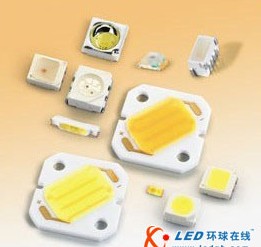
Chip design
From the evolution of the chip, it is found that major LED manufacturers continue to improve on the upstream epitaxial technology, such as using different electrode designs to control the current density, using ITO thin film technology to make the current distribution through the LEDs evenly distributed, etc., so that the structure All produce as much as possible. Then use a variety of different methods to extract each photon emitted by the LED, such as the production of chips of different shapes; use the periphery of the chip to effectively control the light refraction to increase the LED yield, and develop a single chip surface size (> 2mm2) to increase the luminous area It also uses a rough surface to increase the penetration of light and so on.
There are some high-brightness LED chips on which the positions of the two electrodes of pn are close to each other, which improves the luminous efficiency and heat dissipation capability of the chip. Recently, the existing production is to remove the LED epitaxial wafer from the GaAs or GaN long crystal substrate and bond it to another metal by using the newly improved laser lift-o and metal bonding. On the substrate or other materials with high reflectivity and high thermal conductivity, it helps high-power LEDs to improve light extraction efficiency and heat dissipation.
Package design
After years of development, vertical (φ3mm, φ5mm) and SMD lamps (surface mount LEDs) have evolved into a standard product model. However, with the development and needs of the chip, we have developed a package design that meets high power. In order to reduce manufacturing costs by using automated assembly technology, high-power SMD lamps have emerged. Moreover, driven by the rapid market of portable consumer products, the design of high-power LED package volume is smaller and thinner to provide a wider product design space.

In order to maintain the brightness of the finished product after packaging, a new modified high-power SMD device with a cup-shaped reflecting surface helps to reflect all the light out of the package to increase the output. Covering the round shape of the LED, the material is changed to use Silone sealant instead of the epoxy resin (Epoxy), so that the package can maintain a certain durability.
Packaging process and solution
The main purpose of the package is to ensure the correct electrical and mechanical interconnection between the semiconductor chip and the underlying circuit, and to protect the chip from mechanical, thermal, humid and other external impacts. When selecting the packaging method, materials, and operating the machine, factors such as the shape of the LED epitaxial, electrical/mechanical characteristics, and the accuracy of the die attach must be considered. Due to the optical properties of LEDs, packaging must also be considered and ensured in optical properties.
Whether it is a vertical LED or SMD package, a high-precision die bonder must be selected. The accuracy of the LED die placed in the package directly affects the luminous performance of the package. If the position of the crystal grains in the reflective cup is deviated, the light is not completely reflected, which affects the brightness of the finished product. However, if a solid crystal machine has an advanced PR System, it can be accurately soldered to a predetermined position in the reflector despite the poor quality lead frame.
Generally, low-power LED devices (such as the illumination of pointing devices and mobile phone keyboards) are mainly solid crystals with silver paste. However, since the silver paste itself cannot withstand high temperatures, while the brightness is increased, heat is generated, which affects the product. In order to obtain high-quality and high-power LEDs, a new die-hardening process has been developed. One of them is to use eutectic soldering technology to solder the die to a heat sink (soubmount) or heat sink. Then, the whole die is connected to the heat dissipating substrate and then soldered to the package device, so that the heat dissipation capability of the device can be enhanced, and the hair is relatively increased. As for the substrate material, silicon (Silicon), copper (Copper) and ceramic (Ceramic) are commonly used heat-dissipating substrate materials.
Eutectic soldering
The most critical technology is the choice of eutectic materials and the control of soldering temperature. A new generation of InGaN high-brightness LEDs, such as eutectic soldering, can use pure tin (Sn) or gold-tin (Au-Sn) alloy as the contact surface coating on the bottom of the die, and the die can be soldered to the substrate coated with gold or silver. on. When the substrate is heated to a suitable eutectic temperature, gold or silver elements penetrate into the gold-tin alloy layer, the composition of the alloy layer changes to increase the melting point, the eutectic layer is cured and the LED is soldered to the heat sink or substrate. .
The choice of eutectic temperature depends on the heat resistance of the die, substrate and device materials and the temperature requirements of the subsequent SMT reflow process. When considering the eutectic solid crystal machine, in addition to high positional accuracy, another important condition is flexible and stable temperature control. Nitrogen or mixed gas devices are added to help prevent oxidation during the eutectic process. Of course, like the silver paste solid crystal, to achieve high-precision solid crystal, relying on rigorous mechanical design and high-precision motor movement, the welding head and welding force control can be just right, and the high productivity and high yield rate are not damaged. Requirements.
Flux can also be added during the eutectic soldering process. The biggest feature of this technology is that no additional soldering force is required, so there is no excessive eutectic alloy overflow due to excessive bonding force, which reduces the chance of LED short circuit. .
Flip Chip soldering
Flip chip soldering has been actively used in high-power LED processes in recent years. The flip chip method has fused the GaN LED die to the heat-dissipating substrate. Because there is no gold wire pad hindrance, it will help to improve the brightness. Since the distance through which the current flows is shortened and the resistance is reduced, the generation of heat is relatively lowered. At the same time, such bonding can effectively transfer heat to the heat sink substrate of the next layer and then go outside the device. When this process is applied, not only the light output is increased, but also the overall area of ​​the product can be reduced, and the application market of the product can be expanded.
There are two main options for the development of flip chip LED technology: one is the Solder bump reflow technology; the other is the Thermosonic soldering technology.
Lead solder ball soldering has been used in IC packaging applications, and the process technology has matured, so it will not be described in detail here. Thermosonic flip chip technology is especially suitable for high power LED soldering for the production of low cost and low line devices. Gold is used for welding. Because the melting temperature of gold is higher than that of lead-tin balls and silver paste, it is more flexible in the process design after solid-crystal.
In addition, there are advantages such as lead-free process, simple process, and reliable metal connection. After many years of research and experience accumulation, the thermosonic flip chip process has mastered the optimized process parameters, and has been successfully put into mass production in several major LED manufacturers. In addition to the use of the production line, the rest of the automation equipment (such as chip bonding machine, wire bonding machine, machine, tape machine) and other automation equipment are all dependent on imports.
For the 66kV Oil Immersed Power Transformer, we can produce capacity upto 180MVA. We use the best quality of raw material and advance design software to provide low noise, low losses, low partial discharge and high short-circuit impedance for power transformer.
Our power transformer are widely used in national grid, city grid, rural grid, power plant, industrial and mining enterprise, and petrochemical industry.
Rectifier Transformer,66Kv Power Transformer,66Kv Transformer,66Kv Transformer With Octc
Hangzhou Qiantang River Electric Group Co., Ltd.(QRE) , https://www.qretransformer.com