
The biggest feature of DSP+FPGA architecture is flexible structure, strong versatility, and suitable for modular design, which can improve the efficiency of the algorithm. At the same time, its development cycle is short, the system is easy to maintain and upgrade, and it is suitable for real-time video image processing.
The system adopts a modular design method and divides the whole system into three parts: video acquisition unit, video processing unit and video transmission unit.
The whole system uses FPGA as the core control unit and completes the median filtering of the video signal. The DSP is used as the core processing unit of the whole system to perform JPEG compression on the captured video image information. In the video transmission unit, the USB based on PDIUSBD12 chip is designed. The bus is responsible for the transmission of video signals.
1 system hardware architecture
A complete video processing system is mainly composed of a video acquisition unit, a video processing unit and a video transmission unit. Make sure that the parts are seamlessly connected when designing the system.
The image acquisition unit is composed of FPGA and MB86S02 video acquisition chip, including video signal acquisition and preprocessing, converting the input video signal into digital image data that the system can process, and storing it in a certain storage area according to a certain format.
The image processing unit is the core of the system, and compresses the image data to realize the functions that the system has to achieve.
The image transmission unit uses FPGA+USB to realize the transmission of video data. The compressed video image information is sent to the receiving end through the USB bus based on the PDIUSBD12 chip, and the image is decompressed at the receiving end by using an application written on the PC. And show it.
The whole hardware system is composed of two sub-systems, FPGA and DSP. As a video acquisition unit, the FPGA preprocesses the acquired video signal and transmits it to the DSP. The DSP as the image processing unit is the core of the system, and the pre-processed video of the FPGA. The image information is processed by JPEG compression. The performance of the DSP unit determines the performance of the whole system. After the DSP completes the image processing task, the result will be returned to the FPGA. The FPGA writes the compressed image information to the data buffer of the interface control chip. The interface control chip is responsible for the transmission of information. The overall block diagram of the system is shown in Figure 1.
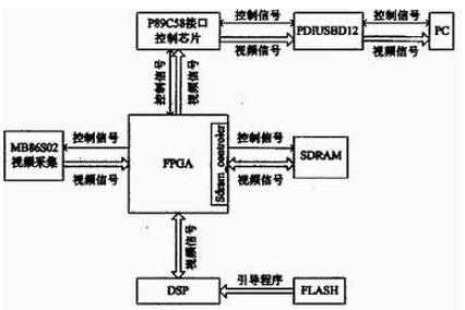
Figure 1 Overall structure of the system
As shown in Figure 1, the MB86S02 video image sensor collects video image information under the control of the FPGA. After receiving the acquisition command from the PC, MB86S02 starts the acquisition of the video signal. The FPGA is the core control unit of the system, not only responsible for the video image acquisition. And responsible for the preprocessing of video image information and data interaction between the various unit modules of the system.
In order to ensure the real-time requirements of the system, the system uses a large-capacity off-chip SDRAMR to cache the captured video image information. The SDRAM controller is implemented by FPGA, and the video image information is first buffered by SDRAM. To be filtered by the FPGA to eliminate noise interference in the image information, the system uses median filtering to process the collected video information, and the filtered data enters the DSP through the FPGA internal FIFO for the next step. Compression processing. After the DSP is powered on, the boot program is self-loaded, waiting for the FPGA to send a request. After receiving the FPGA request, the DSP establishes an EDMA channel to acquire video data from the FPGA. After storing one frame, the video image is subjected to JPEG compression processing. After the compressed video image information is buffered by the FIFO, it is written into the data buffer area of ​​the USB interface controller under the control of the FPGA, waiting for the reading request of the PC, and the USB interface controller sends the data after receiving the reading request from the PC. Write to port 1 of PDIUSBD12 so that the PC can read the data in the next step.
2 system software overall design
The software design of the system can be divided into two parts according to the overall division of the hardware structure. The operation of the whole system is shown in Figure 2. The respective programs of the FPGA and DSP run independently, and the real-time interaction of data is completed by the interrupt signal. The instruction from the FPGA to the DSP is to send an EDMA request through the FPGA. The DSP establishes an EDMA channel by responding to the EDMA request, and starts reading the data from the FIFO after preprocessing. When the DSP transmits data to the FPGA, it sends an interrupt to the FPGA. The signal is read out from the FIFO by the compressed image data.
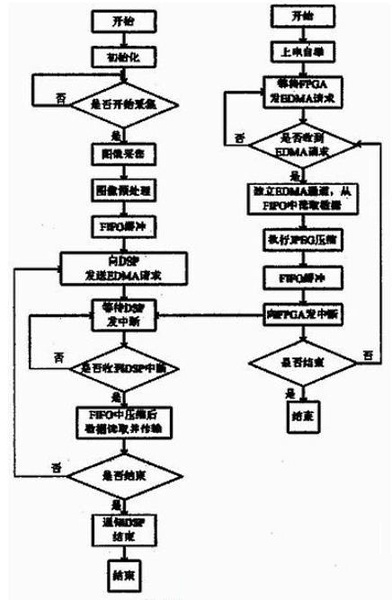
Figure 2 system software software flow chart
As shown in Figure 2, the whole system workflow can be briefly described as follows: After the system is powered on, the DSP first bootstraps by flash and runs the boot program, then transfers to the EDMA wait state, and waits for external image acquisition commands after the FPGA is initialized. After the image acquisition command, the image acquisition is started, and the acquired image is preprocessed. The preprocessed image is buffered by the FIFO. After storing a certain amount of data, the FPGA sends an EDMA request to the DSP through the half full signal, waiting for the DSP. In response, once the DSP receives the EDMA request from the FPGA, it immediately establishes the EDMA channel, reads the data from the FIFO to the L2 memory, and after the image is full, the DSP begins image compression. After waiting for an image to be compressed, the DSP will go to the FPGA. The interrupt signal is sent, and the FPGA starts to read the compressed image data from the FIFO after receiving the interrupt signal. After reading one frame of data, it is judged whether the encoded signal is valid. If it is valid, the next frame image is compressed according to the same rule, and if it is invalid, the DSP is notified to end.
This design has been verified by hardware, meets the predetermined design requirements, and realizes real-time processing of large amounts of data.
The system volume is only 70 & TImes; 70mm, the power consumption is less than 5W, the median filtering rate is 20F/S on average, and the JPEG compression rate is above 25F/s. Not only meets the real-time requirements of the video processing system, but also has small size, low power consumption, and FPGA-based programmability, the system has good flexibility and scalability.
Integrated Rimless LED Panel Light includes round and square two shape frame. We are the manufacturer of producing energy saving interior lighting. These trimless led panels has built-in driver and external driver. The frame shell is made of PC material. There are three color temperatures with cool white, warm white and natural white of panel lights. It has both concealed and surface mounted installation way. The unique features of led trimless light are: CRI>80, PF>0.5. These panels are mainly apply to home, office and school, etc.
Integrated Rimless Concealed Mounted Led Panel Light
Led Panel rimless Light,Interior Led Integration Light ,Led Integrated Light ,Round Rimless Integrated Lamp
Jiangmen Lika Lighting Electrical Appliances Co., Ltd , https://www.lika-led.com