
Design of automotive electronics based on FPGA
1 Introduction With the advancement of digital technology, automobiles are beginning to develop in the direction of electronics, multimedia and intelligence. More and more electronic technologies are applied to automobile systems. The degree of automobile electronics is an important indicator of the level of modern automobiles and is The most important technical measures to develop new car models and improve car performance. According to statistics, the current cost of electronic devices in automobiles accounts for about 30% of the total vehicle cost, reaching 60% in some high-end cars, and about 70% of innovations in automobiles come from automotive electronic technology. In the past, automotive engineers have relied on MCU (microcontroller) and ASIC (application specific integrated circuit) products to design automotive electronic systems, but as the system becomes more complex and the number of components increases, the pressure to quickly bring products to market becomes greater The performance requirements are gradually increasing. At the same time, the price must be reasonable and the design risk should be low. These are difficult to achieve by MCU and ASIC. And FPGA can provide higher performance and more functions, lower cost, less risk, higher flexibility, and more easily change in the later stage of the design, and even upgrade products that have been put into application, so FPGA will become The ideal solution for future automotive electronics design.
2 Introduction to FPGA Field Programmable Gate Array FPGA (Field Programmable Gate Ar-ray) is the product of the development of programmable devices such as PAL, GAL, CPLD, and is a semi-custom circuit in the field of special integrated circuits. It is composed of three parts: Configurable Logic Block (CLB), IOB (Input Outout Block) and Interconnect (Interconnect). It has miniaturization, low power consumption, multi-function, digitization, standardization and series. It has the characteristics of high degree of integration, high integration, good confidentiality, can be programmed repeatedly, and has the characteristics of on-site simulation debugging verification. Altera and Xilinx use RAM technology to produce general-purpose FPGA; Actel provides non-volatile FPGA based on anti-fuse technology and Flash technology.
3 Application of FPGA in the design of automotive electronics Based on these characteristics of FPGA, more and more domestic and foreign research on its application in the design of automotive electronics has become more and more. A foreign company has begun to introduce FPGA devices into its engine control system design. There are also a lot of FPGA-based automotive electronic designs in China, such as FPGA-based ABS system design, automotive electronic rear-view mirror system design, CAN bus communication system design based on Nios II, automotive anti-theft system based on GSM / GPS and based on SoPC's automotive instrument system design, etc. The parallel processing method of FPGA has a high processing speed, and is widely used in car audio and video processing. With more and more car infotainment system functions, such as GPS navigation system, video and audio playback function, reversing image system, car TV function, FM radio, MP3 playback function, etc., this requires the system to have higher audio and graphics The processing power requires a lot of calculation and is implemented by high-end processors and DSPs, but the system cost, complexity and power consumption are high. Car voice processing module mainly involves digital processing of voice, voice encoding and decoding, voice compression and voice recognition technology. In particular, voice recognition systems need to process and sample sounds in real time, but the cost of implementing the above methods is very high, which is not desirable for the cost-sensitive automotive industry, and FPGA can solve these problems because it can be in one clock cycle Processing multiple instructions to achieve parallel computing, high computing power, able to complete video and audio processing tasks. In addition, FPGA also has corresponding applications in automotive data acquisition and hardware-in-the-loop (HIL) simulation of electronic control units (ECU).
Secondly, it can reflect its high flexibility, high integration, high performance, and short development cycle in system design. For example, adopting the FPGA design system of Ahera, by calling the corresponding IP core in SoPC Builder, you can control the memory such as SDRAM, Flash and a variety of automobile common interfaces, and realize the hardware circuit connection and control of the single device and each module. Thereby greatly improving the integration and development efficiency of the system. In addition, because audio and video processing requires FPGAs with high computing processing capabilities, Ahera has FPGA devices that support multiple CPUs, that is, multiple Nios II soft core processors, so that modules that require high processing speed such as audio and video processing Separated from the main CPU to reduce the processing load of the main CPU, enhance the stability of the system, and save costs.
4 FPGA-based automotive electronics design
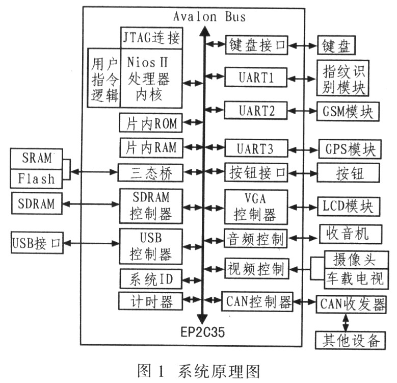
4.1 System design system FPGA device selects EP2C35F672C8N of Ahera's Cyclone II series. The system design implements code lock and fingerprint recognition, GPS navigation, GSM communication, auto anti-theft alarm, reversing image and in-car camera, radio, car TV , USB data transmission and other functions, in addition to the CAN bus controller interface, it is convenient for subsequent system development. The system design uses programmable on-chip system SoPC (System On Programmable Chip) technology to integrate processors, memory, I / O ports and other modules into a programmable device to form a programmable system-on-chip. The system designed in this way achieves the best in many aspects such as scale, reliability, volume, power consumption, function, performance index, time to market, development cost, product maintenance and hardware upgrade. Use Quartus II SoPCBuilder and Nios II IDE 3 software combination to complete system design and debugging. In the design process, for relatively simple control (such as password lock module), you can directly write Verilog code in Quartus II, simulation optimization, pin assignment and finally generate the module; for relatively complex module control, create a project in Quartus II, and then open Sopc Builder builds a system. Figure 1 is a schematic diagram of a hardware system built using SoPC Builder. After the system is set up, address allocation and system simulation are performed, and finally the system module is generated. Then, the system software is developed in the Nios II IDE environment to complete the system software development. Finally, the Quartus II is connected and assigned pins, simulation, testing, compiling and generating download files , Download to FPGA device through JTAG interface, complete system development.
4.2 System module design
4.2.1 Combination lock and fingerprint identification These two modules are mainly used to strengthen the anti-theft safety factor of the car. The two modules can be activated at the same time or individually. When one of them is verified independently, no changes can be made to the system. Only two modules can pass the verification at the same time to set up the system.
The password lock module uses any 6 numbers from 0 to 9 as the system password. The design principle of the module is shown in Figure 2. This module mainly includes a keyboard. Password verification and result output. Among them, the keyboard is realized by using Verilog language programming in the Quartus II environment, and its program is composed of clock frequency division, keyboard scanning and key decoding conversion. In the two modules of password verification and result output, when the user enters the password through the keyboard, the password and the output result are displayed with "*" on the LCD, which is completely realized by Verilog programming.
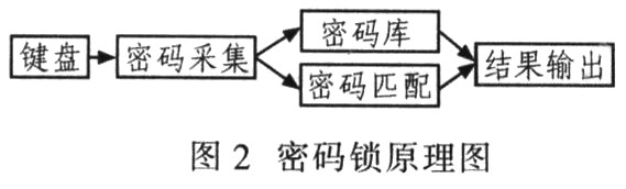
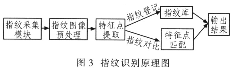
Figure 3 is a schematic diagram of the fingerprint identification module design. Collect the fingerprint through the fingerprint collection module, input the data to the FPGA device through the serial port for image preprocessing, convert it into a digital image with a certain gray level, and then extract the feature points. Compared with the fingerprint image in the fingerprint library, the comparison result is finally output. This module is designed and implemented using Nios II processor.
4.2.2 GPS navigation module To construct a GPS navigation system, you need a GPS antenna, a receiving module, a memory, a processor, a corresponding control button, and a map LCD display device. In order to improve the development cycle, the system directly uses GARMIN's GPS25 OEM development board. The connection circuit between it and FPGA development board is shown in Figure 4.
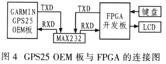
This GPS module converts the serial port signal level through the MAX232 device, and then connects to the serial port of the development board to realize the construction of the hardware system. The system software is designed to read GPS information using C programming under the NiosIDE environment, extract GPS coordinate information and import it into the map software stored in the memory, and display navigation images on the LCD through the LCD control module. To realize the design of GPS navigation module
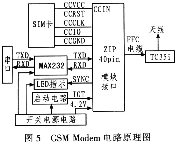
4.2.3 GSM communication module The system requires high stability and high anti-interference performance. So choose Siemens TC35i module to build GSM Modem circuit (GPRS module + SIM card + power conversion + RS232 interface), as shown in Figure 5. Directly connect the GSM Modem module to the FPGA through the serial port, and then through programming, send AT commands through the serial port of the FPGA development board to control the GSM module.
4.2.4 Vehicle-mounted anti-theft system The vehicle-mounted information device is equipped with GPS positioning equipment and GSM communication equipment, so it can monitor the vehicle in real time. Separate the GPS from the on-board information device and place it in a hidden place together with GPRS, equipped with an independent power supply. After the car is stolen, it can send SMS instructions to the GSM module through the mobile phone or network, and send the real-time coordinates of the car determined by the GPS module and the captured image of the camera inside the vehicle to the user through the GPRS network connected to the GSM module In places, it is necessary to determine the approximate location of the car through the GSM positioning of the mobile company. You can also control the relay by sending commands to the GSM module. In turn, control of car engines, fuel supply systems, ignition systems and other equipment is conducive to controlling vehicles and finding stolen vehicles in time to reduce losses.
4.2.5 Other module design The radio module of the system uses TEA5768HL device, the car TV module uses Philips video electronic tuner, and the CAN bus controller uses SJA1000 main control device and AS2C250 auxiliary device to build the port. It can be seen that, simply connect the GSM, GPS, fingerprint, camera and other modules to the development board built by the FPGA device and the corresponding external circuit through the serial port, USB port and other interfaces to complete the establishment of the hardware system. The software system program utilizes many peripheral control IP cores provided by Altera, and designers do not have to write control programs for all peripherals from scratch, which can improve design efficiency and shorten development cycles.
5 Conclusion FPGA realizes the multi-module centralized control of automotive electronics, enhances the flexibility of automotive electronics design, shortens the development cycle, lowers the cost, reduces the space occupied by the electronic system in the car, and at the same time improves the stability and ease of maintenance of the system, which is convenient System Upgrade. Therefore, FPGA will definitely have outstanding performance in the future automotive electronics design.
The 6KV/6.6KV Medium Voltage Variable Frequency Drive is a product accumulated by FGI for over 20 years. The system adopts modular design, mainly including phase shift transformer cabinet, power unit cabinet and control cabinet, etc. The Mv Vfd has the advantages of low input harmonic content and high power factor. The High Voltage Drive is widely used in pumps, fans, woodworking machinery, cement production and other industries.
6Kv And 6.6Kv Medium Voltage Drives
Mv Drives,Mv Vfd,High Power Motor Drives,6Kv And 6.6Kv Medium Voltage Drives,Medium Voltage Motor Starter,High Voltage Motor Controller
FGI SCIENCE AND TECHNOLOGY CO., LTD , https://www.fgi-tech.com