
Research and Design of FED Matrix Scanning Power Amplifier Circuit
Field emission display (Field Emission Display, FED) is a new type of flat panel display device, considered to be the most likely flat panel display to compete with plasma (PDP) and liquid crystal display (LCD), it has a fast response speed, The advantages of light weight, low power consumption, large viewing angle, bright colors, etc. meet the requirements of consumers for display quality, and have considerable market prospects. The principle of image generation by FED is the same as that of cathode ray tube (CRT), all of which emit light by bombardment of phosphor, but the matrix addressing method is adopted. FED drive circuit is the top priority of FED research and development. Fuzhou University has developed a 25-inch color large screen with independent intellectual property rights for low-escape with the support of the National Ministry of Science and Technology, local related science and technology departments and many large domestic enterprises. Power-printed field emission display. According to the characteristics of FED matrix addressing, the corresponding matrix scanning power amplifier circuit is designed, including discrete and integrated drive and hybrid drive circuit combining discrete and integrated advantages. These circuits have been used in 25-inch QVGA, VGA FED, and will be further applied in 34-inch FED drive circuit.
1 Features of FED matrix scanning power amplifier circuit
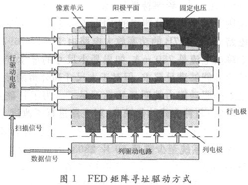
As shown in Figure 1, FED, like most flat panel displays, also uses a row and column matrix addressing driving mode of operation, the anode is applied with a fixed voltage, the gate is used as a row electrode, and the cathode is used as a column electrode. Pixel unit. The anode voltage is determined by the working voltage required by the phosphor. The row electrode is added to the scan voltage row by row or interlaced, the column electrode is added to the video image signal, and the row and column voltage difference generates field electron emission. Pink glow. The function of the row electrode is to address the scan, and during the row scan, the current of all the columns is collected to provide the power consumption required by the system. For a VGA system, the design goal is that the column drive voltage pulse amplitude is 100 V, the current pulse amplitude is a maximum of 6 mA, and the maximum current collected during electron emission is 3.84 A. For higher resolution systems, this value It will be even higher, which puts forward requirements for large current and relatively large voltage (100-200 V) for the gate high-voltage power amplifier circuit. This requires full consideration of the voltage and current requirements when selecting high-voltage drive transistors or MOS transistors, and the stability is quite good. It is more difficult for integrated circuits to meet this requirement. Because of the limitations of the manufacturing process of integrated circuits, there is no special chip developed for FED drive current on the market. Based on the PDP circuit design method, a PDP dedicated chip STV7696B line integrated system.
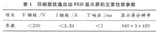
The measured value of the work function of the FED cathode is about 2 eV, the typical emission current of the experimentally tested FED cathode is about 3 mA / pixel, and the minimum cathode emission area is O. 4 mm × O. 4 mm. Table 1 is the main performance parameters of the printed FED display.
2 Discrete matrix scanning power amplifier circuit
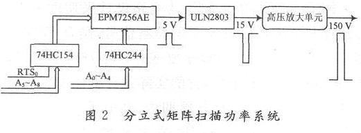
Based on the discrete matrix scanning power system, the CPLD programmable device completes decoding the row signals provided by the main board, and then passes through the power amplification of the high-voltage MOS tube to complete the entire system. The system block diagram is shown in Figure 2.
The high-voltage power amplifying part must not only further raise the low-voltage scanning pulse of the previous stage, but also provide the current load capacity, so as to provide sufficient current for the gray-scale display of the column power system. The current provided by general transistors and MOS tubes is only a few hundred milliamperes, which may be insufficient for the system, so power MOS tubes are the best choice for this design.
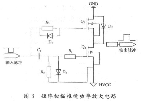
As shown in Figure 3, a push-pull circuit composed of a power MOS tube is used, and the low-voltage scan pulse enters the high-voltage drive unit for amplification. When the circuit works, the two symmetrical power switch tubes only have one conduction at a time, so the conduction loss is small and the efficiency is high. The parameters of MOS transistors Q1 and Q2 in Fig. 3 are the same, and they exist in the circuit in a push-pull manner. When the pulse is high, the Q1 tube is turned on, the Q2 tube is turned off, and the circuit outputs a low level; when the pulse is low, the Q1 tube is turned off, the Q2 tube is turned on, and the circuit outputs a high level. Through the mutual conduction of the two MOS tubes, the power consumption is reduced, and the bearing capacity of each tube is improved, which is suitable for the FED driving large current requirements. The parallel clamping circuit composed of resistor R2 and diode D3 aims to accelerate the conduction speed of MOS.
3 Integrated matrix scanning power amplifier circuit
3.1 Introduction to STV7697B
STV7697B is a scan driver chip dedicated to PDP produced by ST. It has a 64-bit cascade shift register with a frequency of up to 8 MHz, which can realize 64 high-voltage high-current outputs. Through cascading, arbitrary vertical pixels can be realized. The logic control of the low-voltage part uses a voltage of 5 V, and the maximum power supply voltage of the high-voltage part is 170 V. All inputs are compatible with CMOS. STV7697B also has the following features:
(1) The peak output current is 200/750 mA;
(2) The maximum source output current is 1 A;
(3) Blanking signal control;
(4) Complementary output control;
(5) 100-pin TQFP package.
3. 2 STV7697B driving scheme
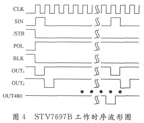
Figure 4 is the working timing waveform of the chip. During operation, the SIN pin receives the scan signal sent from the control board. The polarity transmission direction selects the control terminal F / R to select the transmission direction. The signal shifts at the instant of the rising edge of the line synchronization clock CLK. The bit register shifts forward, and the data of the shift register is placed in the latch under the control of STB. When the BLK is allowed to output, the signal passes through the internal power amplifier gain to output the corresponding high-voltage signal.
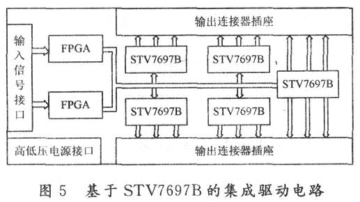
FED matrix scan integrated drive circuit design uses FPGA chip control to generate the control signals required for row drive, combined with the internal structure and timing requirements of the STV7697B chip. STV7697B can be used in cascade to achieve matrix scan output. Its actual design block diagram is shown in Figure 5. When the line circuit is working, during each line period, the high-level active SIN signal is input from the SIN terminal of the first STV7697B, output from the SOUT terminal of the chip, and then cascaded with the SIN terminal of the latter chip. In this way, in the period of the line scan pulse CLK signal, the scan data level is sequentially shifted from the first output to the last output, and each signal outputs the scan pulse of the corresponding line through the internal power amplifier gain and is loaded on the FED display Row electrode.
3. 3 STV7697B software design
According to the requirements of the FED system, such as the VGA system, the time to scan one line is 64 μs. The signal transmitted from the main board is an 8-bit address signal and a parity field identification signal. The 8-bit address signal is obtained by frequency division and has the shortest cycle The signal a [O] period is 64μs, which can be triggered by the rising edge. When the parity field signal RTSO is low, when the rising edge of a [0] comes, let SIN = 1, CLK = a [0], clear the signal CLR is low, at the same time counter n starts to count, a [0] Every time a rising edge comes, n is increased by 1, when n> 1, SIN = 0; and when RTSO is high, the clear signal is high, while another The field began to work. Among them the signal / STB, POL, BLK and F / R are all output by FPGA setting value. Within the time of one frame of image, the scan clock is scanned from the first line to the 480th line. When the next frame arrives, the previous process is repeated.
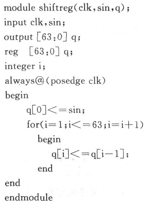
The high voltage output part is in principle a 64-bit shift register, and its procedure is as follows:
4 Hybrid matrix scanning power amplifier circuit
Two matrix scanning power amplifier circuits have been studied above. Among them, the circuit composed of discrete components has low conduction loss, high efficiency, strong circuit load capacity, high switching speed, and good frequency characteristics. However, its large number of components is difficult to apply to large In the high-resolution FED display. The power amplifier circuit based on the integrated circuit STV7697B because the maximum output current of the STV7697B is 750 mA, if it is a small-size display, this parameter value can still meet the requirements, but for the large-size high-resolution display, its driving ability is Obviously feeling insufficient. In order to break this contradiction, combining the advantages and disadvantages of the two methods, the circuit has been improved. It can be seen from Figure 2 that the output of ULN2803 is only 8 channels at most, and at least 60 2803 are required for VGA system, so if you can replace it with a higher integration chip, you can save more space. The integrated chip STV7697B just meets this requirement. Reasons as follows:
(1) STV7697B high voltage and large current output can completely replace ULN2803;
(2) STV7697B has 64 outputs, while ULN2803 has only 8 outputs, which can greatly save PCB board space;
(3) ULN2803 is only suitable for the case where the gate is a positive voltage, and STV7697B does not have this limitation;
(4) The stability of the system is further improved.
Based on the above analysis, STV7697B was used to replace ULN2803 in discrete systems. After experiments, it satisfactorily met the requirements of FED matrix scanning power amplifier circuits.
5 large screen FED display effect
The display effect of the printed field emission display that has been successfully developed to display video images of 63.5 cm (25 in) is shown in Figure 6.

The main performance of the prototype is as follows:
Display size: 63.5 cm (25 in); color: color; gray level: 256 levels; contrast: 1 010: 1; display resolution: 640 × 480 (VGA); brightness: 410 cd / m2; refresh rate : 60 frames; display content: video image.6 Conclusion
Developed three kinds of FED matrix scanning power amplifier circuits, each of which has advantages and disadvantages. Since there is no special chip developed for the FED drive circuit, the research on the power amplifier circuit suitable for FED drive requirements will lead to the future development of FED. It is of positive significance, and also provides ideas for the production of special integrated circuits in the future. Successfully realized the printed FED video display system that drives the display VGA resolution, can display various color video images, the brightness has reached 410 cd / m2, the contrast ratio has reached 1 010: 1, and the image display quality, system stability, prototype volume, etc Great progress has been made.
Shenzhen Dianjiang Engineering Co. LTD , https://www.isourceled.com