
Abstract: Vast resources have been spent by the semiconductor industry to build high-speed nonvolaTIle random-access read / write memory. This effort was undertaken because NV SRAM offers advantages over other memory devices such as DRAM, SRAM, EEPROM, Shadow RAM, EPROM , and ROM. NV SRAM was developed to meet specific needs of the design engineer. This arTIcle describes applicaTIons requiring this type of memory and compares this memory technology to other memory technologies available.
Vast resources have been expended by the semiconductor industry trying to build a nonvolaTIle random access read / write memory. The effort has been undertaken because nonvolatile RAM offers several advantages over other memory devices—DRAM, Static RAM, Shadow RAM, EEPROM, EPROM and ROM —Which were developed to meet specific applications needs.
Characteristics of the ideal nonvolatile RAM are: low power consumption, high performance, high reliability, high density, low cost, and the ability to be used in any semiconductor memory application.
While the various memory components designed to date do not meet the ideal memory scenario, each excels in meeting one or more of the sought after attributes (Table 1).
Table 1. Memory Attributes
+ = Degree of excellence Types of MemoryMany types of memories have been devised to meet varying application needs. However, nonvolatile read / write random access memories can be substituted for all memory types independent of application, if cost is not a primary consideration.
DRAM: Dynamic Random Access MemoryA DRAM, similar to an SRAM, stores information as a 1 or a 0. In an SRAM, this information is stored in a four to six transistor flip-flop which is easy to address, but requires a relatively large memory cell. A DRAM, by comparison, stores its 1 or 0 as a charge on a small capacitor, requiring much more current then an SRAM to maintain the stored data. The net memory cell size is smaller for the DRAM than for the SRAM, so the total cost per bit of memory is less. The DRAM's capacitors must be constantly refreshed so that they retain their charge. DRAMs require more sophisticated interface circuitry.
SRAM: Static Random Access MemoryAn SRAM is essentially a stable DC flip-flop requiring no clock timing or refreshing. The contents of an SRAM memory are retained as long as power is supplied. SRAMs support extremely fast access times. SRAMs also have relatively few strict timing requirements and a parallel address structure, making them particularly suitable for cache and other low-density, frequent-access applications.
NV SRAM: Nonvolatile Static Random Access MemoryAn NV SRAM is a single package which contains a low-power SRAM, a nonvolatile memory controller, and a lithium type battery. When the power supply to this single modular package falls below the minimum requirement to maintain the contents of the SRAM, the memory controller in the module switches the power supply from the external source to the internal lithium battery and write protects the SRAM. These transitions to and from the external power source are transparent to the SRAM, making it a true nonvolatile memory. This unique construction combines the strategic advantages of SRAM—addressing structure, high-speed access, and timing requirements—with the nonvolatility advantages of EEPROM technologies. Battery-backed SRAM modules from Dallas Semiconductor are pin-compatible with non-battery-backed SRAMs, making them ideal for any application where a traditional SRAM would be suitable.
PSEUDO STATIC RAM: Pseudo Static Random Access Memory The advantages of using a Static RAM are the simplicity of the interface circuitry required, and the fact that the device is by nature "static," not requiring periodic refreshing to retain its data. A DRAM, however , provides lower cost-per-bit advantages and a higher memory density. A Pseudo-static RAM combines the advantages of the SRAM and DRAM by using dynamic storage cells to retain memory, and by placing all the required refresh logic on-chip so that the device functions similarly to an SRAM.
FlashA flash memory combines the electrical erase capability of an EEPROM with a cell that is similar to an EPROM. The result is that the modified cell may be block erased electrically instead of with UV light. This feature allows a Flash memory to accept new code updates or information while it is functioning in a system.
EEPROM: Electrically Erasable / Programmable Read Only MemoryA significant disadvantage of the EPROM memory is the fact that it cannot be reprogrammed while in a system. EPROM requires an external programming device to receive new code or data. An EEPROM eliminates this problem by providing a write function which can be used while the EEPROM is still in a circuit. A tradeoff for obtaining the write function while the EEPROM is still in a circuit is having to provide a high voltage (12.5V or above) source for the EEPROM when writing new data , or buying a more expensive EEPROM which has a charge pump in its package that allows it to be used with a standard 5 to 7V input. Although nonvolatile, EEPROM memory cells exhibit slow read / write access rates, making them most suitable for systems where performance is not an issue. The other read / write capable memories listed in Table 1 provide the ability to frequently read and write data continuously over their entire lifetimes, in excess of 10 yea rs, while EEPROM memory cells can rarely be rewritten more than 10,000 times. An EEPROM can be placed in a system and accessed as a standard RAM.
EPROM: Electrically Programmable Read Only MemoryAn EPROM is a nonvolatile memory which offers the ability to both program and erase the contents of the memory multiple times. An EPROM must be programmed using a 12.5 volt (or higher) PROM programmer, and then transferred into the system in which it is intended to function. EPROMs can be erased by shining ultraviolet light into the window in the top of the IC package. The process of writing data into an EPROM and then erasing it may be repeated almost indefinitely. EPROMs are usually used for product development, and later replaced with less expensive one-time programmable EPROMs.
OTP EPROM: One-Time Programmable EPROMAn EPROM which can only be written with code / data once instead of multiple times. Generally, OTP EPROMs are less expensive then erasable EPROMs.
ROM: Mask Programmable Read Only Memory. Mask programmable ROMs are the most durable form of memory storage. They are, however, "read only" and offer fairly slow performance. If a design has code / data that is very stable and will not need to be changed, a custom mask for the IC die can be made which will significantly reduce the cost of the ROM. A drawback to using a mask ROM is the significant cost penalty that must be incurred if an error in the code / data being stored forces a mask set change. The OTP EPROM fills the gap between ROM applications (no changes) and EPROMs (frequent changes). Meeting Applications NeedsNMOS DRAM memory provides performance and density, but, on the down side, must be constantly refreshed to retain data . At the opposite extreme are ROMs, offering nonvolatility and density, but lacking the ability to be updated with new data because information is programmed in only once. Between these two are a wide range of devices that fulfill some characteristics of the i deal memory.
Two popular devices, EEPROMs and Shadow RAMs, are designed to emulate a static RAM but also have the ability to retain data after a power loss. But despite their capability to retain data, both EEPROMs and Shadow RAMs fall short of meeting the industry's needs for several reasons.
Most notably, the EEPROM requires a special slow write cycle. The EEPROM's inability to support standard write cycle rates hinders performance in applications where memory is updated immediately as new data is available.
Another problem with EEPROMs is their wear-out mechanisms. These raise longevity concerns due to the limited number of write cycles allowed—sometimes as few as 10,000. If a static RAM with a 200 ns cycle time had this limitation, it would wear out in a mere 20 ms. In an application that requires constant updating, such as the buffer memory of a cashier's checkout terminal or a printer, the EEPROM's wear out mechanism is not acceptable.
Finally, because of the complexity of programming circuits, the cell structure and the special process technology required, the density of EEPROMs has not kept up with industry demands.
In systems requiring store-and-forward data, the memory must provide the desired fast write cycle as well as protection of data in the event of a power loss. Despite the promise of such a memory device and the effort invested by the industry, the ideal memory remains elusive.
To more nearly emulate the ideal memory, Dallas Semiconductor combines its intelligent CMOS control circuitry (DS1210), a lithium energy source, and a very low power SRAM to offer a high density, nonvolatile memory.
Five devices, including the DS1220 (2K x 8), DS1225 (8K x 8), DS1230 (32K x 8), DS1245 (128K x 8), and DS1250 (512K x 8), use this fusion of technologies to provide a nonvolatile random access memory solution in densities up to 4096K bits.
CMOS NV SRAMs currently available have read and write cycle times of 70 ns, which exceeds most system requirements. They are much more robust than EEPROM, because there is no wear-out mechanism or write cycle limitation.
NV SRAMs are also the easiest to use and interface because the pinout configurations are standard throughout the industry. In fact, X8 or bytewide NV SRAMs can be interfaced directly to microprocessors (Figure 1). In addition, CMOS NV SRAMs offer low power in both active and standby modes, a characteristic sought by many designers. In most designs, memories remain in standby much of the time, keeping power consumption negligible. In the standby mode, current drain consists of only of leakage currents in the tens of nanoamperes.
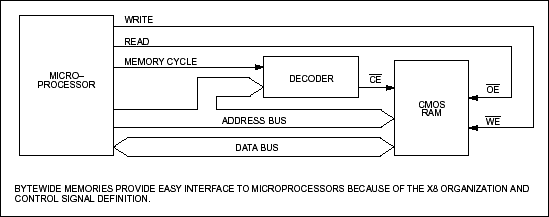
Figure 1. Bytewide RAM to microprocessor interface. Putting Lithium And RAM TogetherThe minute leakage currents of modem CMOS SRAMs can be sustained with a backup energy source to yield a most attractive nonvolatile memory. However, the actual solution involves more than just a CMOS memory and back up energy source (see Figure 2).
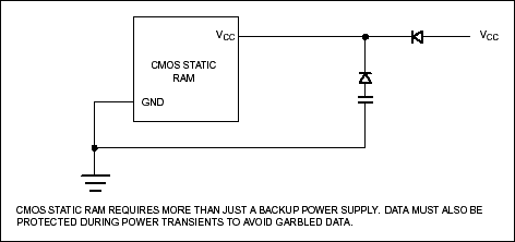
Figure 2. Battery backup circuit.
Battery backup design schemes are many and varied. The increase in density and availability of low-power CMOS memories in recent years has made this approach even more attractive. Yet problems still exist with battery backup design due to battery packaging and a lack of appropriate standard components to implement the support circuitry. One problem is providing isolation between the battery and power supply (see Figure 3). Diodes can provide isolation but produce a voltage drop which requires nonstandard power supplies and also subtracts from the battery voltage. A second problem is that the circuitry must be powered from the battery. Unless these devices draw an extremely modest amount of current, battery selection changes drastically. In fact, a current drain of even a couple of microamperes dictates the use of either rechargeable batteries or a replaceable battery scheme . If rechargeable batteries are selected, the recharging circuit can be costly and complex, and the best rechargea ble battery cannot compare with the electrochemical stability of the lithium primary cell. Even worse, replaceable batteries add maintenance and cost to an in-service system. Battery packaging has also been a serious limitation, taking up valuable space and requiring special handling consideration to prevent discharge.
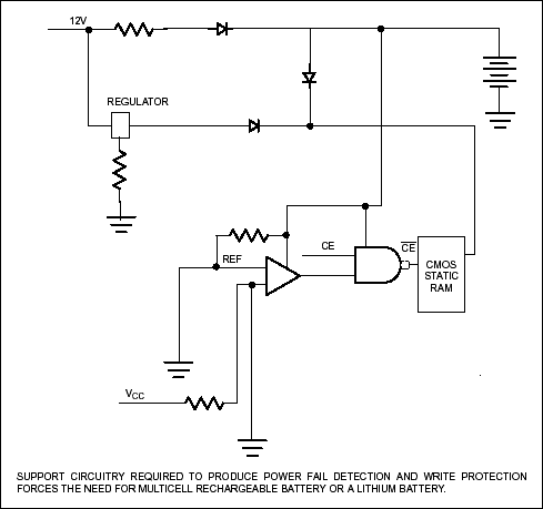
Figure 3. Power supply and battery isolation circuitry.
Dallas Semiconductor overcomes these obstacles by using high-capacity, non-rechargeable lithium batteries in its battery backed SRAMs. Energy SourceThe energy source used to retain data in memory must be capable of outlasting the usefulness of the end product. Dallas Semiconductor NV SRAM products use an extremely stable electrochemical system with enough energy to guarantee a shelf life greater than 10 years. Lithium Battery Backup Is More ReliableThe lithium energy cell has raised concern about reliability and has been the object of much study. Data taken on the energy cell used in Dallas Semiconductor NV SRAMs indicates a cell failure rate less than 0.5% at 55 ° C over a 10 year period.
Additional life studies taken on the same lithium energy source encapsulated in Dallas Semiconductor's NV SRAMs have produced no failures in over 12 million device hours at 85 ° C. The lithium energy cell, then, is ideal for commercial and industrial semiconductor applications. Retrofitting Existing DesignsThe pinout of Dallas Semiconductor NV SRAMs is an established industry standard (Figure 8). The Joint Electronic Devices Engineering Council's Bytewide Version B Standard defines and upgrades from 2K x 8 in density to 128K x 8.
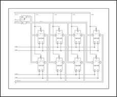
This standard accommodates RAM, ROM, UV EPROMs, and EEPROMs. Because of the flexibility and upgradeability of bytewide memories, the number of existing sockets is in the hundreds of millions. Therefore, many system designs can accommodate direct replacement of RAMs, EPROMs, ROMs , and EEPROMs with Dallas Semiconductor NV SRAMs. These solutions add real-time programmability and / or density upgrades to existing systems without redesign. Real-time programmability gives the system the ability to be personalized by the end user. In other words, NV SRAMs can be retrofitted into existing designs without making changes to existing hardware. This retrofitting offers a cost-effective, practical solution for companies who have invested in other memory devices that are less than ideal for their needs. For example, a design using conventional static RAM can be upgraded to nonvolatile memory by substituting a Dallas Semiconductor NV SRAM for the Static RAM memory. In-Circuit ProgrammabilityThe advanta ges of NV SRAM can be related to the capability of software. Modern systems seek customization for the cost of standard product. In this aspect, software can be adapted in a system to perform specialized functions. It is even possible to totally modify a system personality Over the telephone. In-circuit programming also reduces maintenance cost by eliminating service calls to update software. Software stored in NV SRAM can be updated as often as necessary, depending on the configuration or application of the system. Portable Applications The advancement of high density, low-power portable computers is continuing to drive development requirements. Difficult interface circuitry and refresh requirements of DRAM memories make them unsuitable for such applications. SRAMs are not only easier to address and consume less power when operating, but also require very little power to maintain the contents of their memory. Even better, an NV SRAM can provide the high performance of a DRAM or SRAM an d also guarantee that the memory is truly nonvolatile. When a portable PC needs to be in standby mode, the memory can be powered down altogether. 1 MByte Memory Subsystem Using NV SRAMs Figure 5 shows a system block diagram with an Intel 386SL microprocessor with a 1 megabyte main memory of 128K x 8 NV SRAMs (DS1245). Figure 4, Portable Applications: Intel 386SL CPU / NV SRAM Timing, shows the requisite timing for the memory subsystem. The Intel 386SL is one of many microprocessors specially designed for low power, portable applications, and for addressing SRAM memory.
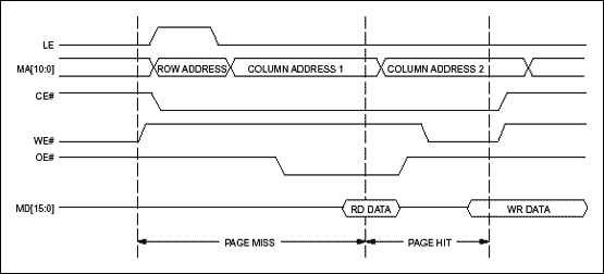
Figure 4. Portable applications: Intel 386SL CPU / NV SRAM timing.
For Larger Image
Figure 5. 1 MByte memory subsystem using NV SRAMs.
In Figure 5, eight DS1245 SRAMs are used to create a four-bank 1Mbyte SRAM memory subsystem. The following signals from the Intel 386SL CPU are required to address the SRAM module based system. (The 386SL memory controller must be configured in its SRAM addressing mode for this application.)
LE: Latch EnableThis signal is active high and serves to indicate that a row address is to be put on the address bus. A row address must be latched at this signal's falling edge. LE is connected to the latch enable input of the address latch.
MA [10: 0]: Multiplexed Memory Address BusThis bus provides address information for the Memory Controller Unit. The bus provides a 22 bit address in a multiplexed row / column sequence.
Active-Low CE [3: 0]: Chip Enable outputsThese signals provide chip enable control for each SRAM bank.
Active-Low WLE: Write Low EnableIndicates a write access to the lower byte of the 386SL CPU memory bus. The lower byte of data is put on the memory bus at the falling edge of Active-Low WLE.
Active-Low WHE: Write High EnableIndicates a write access to the high byte of the 386SL CPU memory bus. The high byte of data is put on the memory bus at the falling edge of Active-Low WHE.
Active-Low OLE: Output Low EnableEnables the lower byte output from the NV SRAM modules.
Active-Low OHE: Output High EnableEnables the high byte output from the NV SRAM modules.
MD [15: 0]: Memory Data BusThis bus provides data information for the Memory Controller Unit. Accesses from the Memory Controller Unit to the NV SRAM memory modules take place through this bus. 16-Bit Single-Bank NV SRAM BIOS CircuitFigure 6 shows Dallas NV SRAMs providing BIOS memory storage for an Intel 386SL CPU. Using the DS1645 NV SRAMs provides several advantages over using either OTP EPROM or FLASH memories.
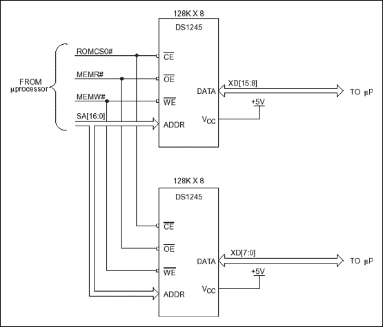
Figure 6. 16-Bit single-bank NV SRAM BIOS circuit.
Flash memories require more operating current than NV SRAMs. Flash memories also require a high voltage source, 12V +, for any writes or updates that must be made to BIOS. NV SRAMs, on the other hand, require only their standard VCC 5V input for both read and write access. Like Flash memories, a DS1645 NV SRAM maintains the contents of its memory in the absence of VCC. A DS1645 has the additional feature that it can be easily programmed to write protect user-selected blocks of memory. In effect, individual memory blocks in the NV SRAM module can be configured to appear as ROM memory, without detracting from the DS1645's ability to receive BIOS updates in its non-write-protected blocks of memory.
Traditional OTP EPROMs, while nonvolatile and very low-power like the DS1245 NV SRAMs, are lacking in that they can only be programmed once, and usually require a special fixture to be programmed. DS1245 NV SRAMs provide the capability to update BIOS repeatedly without removing them from the system. DS1245 NV SRAMs also provide fast 70 ns access times, negating the need to insert additional wait states into BIOS access timing requirements.
The signals shown in Figure 6 are taken directly from the Intel 386SL CPU:
ROMCSO # This signal is a dedicated ROM control signal provided by the 386SL CPU. It is active low and is used to enable the system BIOS.
MEMR #: Memory ReadThis signal indicates when a memory read access is occurring on the ISA bus and is active low.
MEMW #: Memory WriteThis signal indicates when a memory write access is occurring on the ISA bus and is active low.
XD [15: 0]: X-bus DataBuffered data lines from the system data bus. These signals are produced using an external transceiver (see Intel 386SL Superset System Design Guide).
SA [16: 0]: System Address BusThis bus is driven by the 386SL CPU for system I / O accesses. Data LoggingFigure 7 shows how Dallas Semiconductor's NV SRAMs can provide a special advantage in environments where the power supply is not entirely reliable, or when power must periodically be shut down. Dallas Semiconductor NV SRAMs contain memory control circuitry which not only maintains the data in the SRAM in the absence of power, but also write protects the device if VCC is out of tolerance. This feature ensures that an unstable power supply does not corrupt data which has been collected.
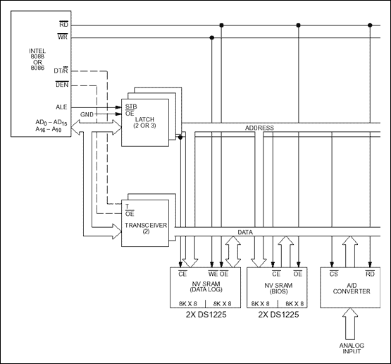
Figure 7. Data logging.
In this application, an Intel 8086 is shown in its minimal mode, connected to an address latch and bus transceiver to demultiplex the 8086's bus (see Figure 7). The resulting address and data busses may then be connected directly to two memory banks, one 8K x 16 BIOS memory consisting of two DS1225 NV SRAMs, the other an 8K x 16 memory bank consisting of two DS1225's acting as a data log. A data collecting device, such as an A / D converter, can be addressed as a read- only peripheral device to sample a value and write it to the DS1225 acting as a data log. The DS1225s acting as the data log can transmit their data on the data bus to another peripheral, or may be removed from the system and taken to another location to have the log extracted.
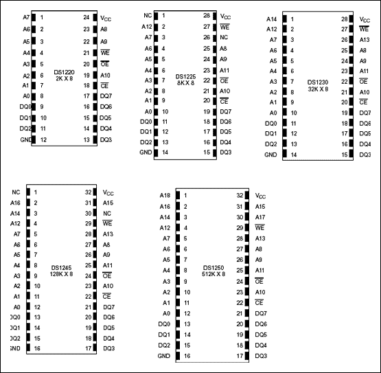
Figure 8. Dallas Semiconductor battery backup SRAM modules.
Vast resources have been expended by the semiconductor industry trying to build a nonvolaTIle random access read / write memory. The effort has been undertaken because nonvolatile RAM offers several advantages over other memory devices—DRAM, Static RAM, Shadow RAM, EEPROM, EPROM and ROM —Which were developed to meet specific applications needs.
Characteristics of the ideal nonvolatile RAM are: low power consumption, high performance, high reliability, high density, low cost, and the ability to be used in any semiconductor memory application.
While the various memory components designed to date do not meet the ideal memory scenario, each excels in meeting one or more of the sought after attributes (Table 1).
Table 1. Memory Attributes
| Cost | Ease Of Interface | Nonvolatile | Density | Performance | Read / Write | Data Retention | |
| DRAM | +++ | +++ | ++ | +++ | |||
| Static RAM | +++ | + | +++ | +++ | |||
| NV SRAM | +++ | ++ | + | +++ | +++ | ++ | |
| PARTITIONABLE NV SRAM | +++ | ++ | + | +++ | +++ | ++ | |
| PSEUDO STATIC | + | + | ++ | + | +++ | ||
| Flash | ++ | ++ | ++ | ++ | ++ | + | ++ |
| EEPROM | + | ++ | + | + | + | + | |
| EPROM | ++ | ++ | ++ | ++ | + | ++ | |
| OTP EPROM | +++ | +++ | +++ | +++ | + | +++ | |
| ROM | +++ | +++ | +++ | +++ | + | +++ |
DRAM: Dynamic Random Access MemoryA DRAM, similar to an SRAM, stores information as a 1 or a 0. In an SRAM, this information is stored in a four to six transistor flip-flop which is easy to address, but requires a relatively large memory cell. A DRAM, by comparison, stores its 1 or 0 as a charge on a small capacitor, requiring much more current then an SRAM to maintain the stored data. The net memory cell size is smaller for the DRAM than for the SRAM, so the total cost per bit of memory is less. The DRAM's capacitors must be constantly refreshed so that they retain their charge. DRAMs require more sophisticated interface circuitry.
SRAM: Static Random Access MemoryAn SRAM is essentially a stable DC flip-flop requiring no clock timing or refreshing. The contents of an SRAM memory are retained as long as power is supplied. SRAMs support extremely fast access times. SRAMs also have relatively few strict timing requirements and a parallel address structure, making them particularly suitable for cache and other low-density, frequent-access applications.
NV SRAM: Nonvolatile Static Random Access MemoryAn NV SRAM is a single package which contains a low-power SRAM, a nonvolatile memory controller, and a lithium type battery. When the power supply to this single modular package falls below the minimum requirement to maintain the contents of the SRAM, the memory controller in the module switches the power supply from the external source to the internal lithium battery and write protects the SRAM. These transitions to and from the external power source are transparent to the SRAM, making it a true nonvolatile memory. This unique construction combines the strategic advantages of SRAM—addressing structure, high-speed access, and timing requirements—with the nonvolatility advantages of EEPROM technologies. Battery-backed SRAM modules from Dallas Semiconductor are pin-compatible with non-battery-backed SRAMs, making them ideal for any application where a traditional SRAM would be suitable.
PSEUDO STATIC RAM: Pseudo Static Random Access Memory The advantages of using a Static RAM are the simplicity of the interface circuitry required, and the fact that the device is by nature "static," not requiring periodic refreshing to retain its data. A DRAM, however , provides lower cost-per-bit advantages and a higher memory density. A Pseudo-static RAM combines the advantages of the SRAM and DRAM by using dynamic storage cells to retain memory, and by placing all the required refresh logic on-chip so that the device functions similarly to an SRAM.
FlashA flash memory combines the electrical erase capability of an EEPROM with a cell that is similar to an EPROM. The result is that the modified cell may be block erased electrically instead of with UV light. This feature allows a Flash memory to accept new code updates or information while it is functioning in a system.
EEPROM: Electrically Erasable / Programmable Read Only MemoryA significant disadvantage of the EPROM memory is the fact that it cannot be reprogrammed while in a system. EPROM requires an external programming device to receive new code or data. An EEPROM eliminates this problem by providing a write function which can be used while the EEPROM is still in a circuit. A tradeoff for obtaining the write function while the EEPROM is still in a circuit is having to provide a high voltage (12.5V or above) source for the EEPROM when writing new data , or buying a more expensive EEPROM which has a charge pump in its package that allows it to be used with a standard 5 to 7V input. Although nonvolatile, EEPROM memory cells exhibit slow read / write access rates, making them most suitable for systems where performance is not an issue. The other read / write capable memories listed in Table 1 provide the ability to frequently read and write data continuously over their entire lifetimes, in excess of 10 yea rs, while EEPROM memory cells can rarely be rewritten more than 10,000 times. An EEPROM can be placed in a system and accessed as a standard RAM.
EPROM: Electrically Programmable Read Only MemoryAn EPROM is a nonvolatile memory which offers the ability to both program and erase the contents of the memory multiple times. An EPROM must be programmed using a 12.5 volt (or higher) PROM programmer, and then transferred into the system in which it is intended to function. EPROMs can be erased by shining ultraviolet light into the window in the top of the IC package. The process of writing data into an EPROM and then erasing it may be repeated almost indefinitely. EPROMs are usually used for product development, and later replaced with less expensive one-time programmable EPROMs.
OTP EPROM: One-Time Programmable EPROMAn EPROM which can only be written with code / data once instead of multiple times. Generally, OTP EPROMs are less expensive then erasable EPROMs.
ROM: Mask Programmable Read Only Memory. Mask programmable ROMs are the most durable form of memory storage. They are, however, "read only" and offer fairly slow performance. If a design has code / data that is very stable and will not need to be changed, a custom mask for the IC die can be made which will significantly reduce the cost of the ROM. A drawback to using a mask ROM is the significant cost penalty that must be incurred if an error in the code / data being stored forces a mask set change. The OTP EPROM fills the gap between ROM applications (no changes) and EPROMs (frequent changes). Meeting Applications NeedsNMOS DRAM memory provides performance and density, but, on the down side, must be constantly refreshed to retain data . At the opposite extreme are ROMs, offering nonvolatility and density, but lacking the ability to be updated with new data because information is programmed in only once. Between these two are a wide range of devices that fulfill some characteristics of the i deal memory.
Two popular devices, EEPROMs and Shadow RAMs, are designed to emulate a static RAM but also have the ability to retain data after a power loss. But despite their capability to retain data, both EEPROMs and Shadow RAMs fall short of meeting the industry's needs for several reasons.
Most notably, the EEPROM requires a special slow write cycle. The EEPROM's inability to support standard write cycle rates hinders performance in applications where memory is updated immediately as new data is available.
Another problem with EEPROMs is their wear-out mechanisms. These raise longevity concerns due to the limited number of write cycles allowed—sometimes as few as 10,000. If a static RAM with a 200 ns cycle time had this limitation, it would wear out in a mere 20 ms. In an application that requires constant updating, such as the buffer memory of a cashier's checkout terminal or a printer, the EEPROM's wear out mechanism is not acceptable.
Finally, because of the complexity of programming circuits, the cell structure and the special process technology required, the density of EEPROMs has not kept up with industry demands.
In systems requiring store-and-forward data, the memory must provide the desired fast write cycle as well as protection of data in the event of a power loss. Despite the promise of such a memory device and the effort invested by the industry, the ideal memory remains elusive.
To more nearly emulate the ideal memory, Dallas Semiconductor combines its intelligent CMOS control circuitry (DS1210), a lithium energy source, and a very low power SRAM to offer a high density, nonvolatile memory.
Five devices, including the DS1220 (2K x 8), DS1225 (8K x 8), DS1230 (32K x 8), DS1245 (128K x 8), and DS1250 (512K x 8), use this fusion of technologies to provide a nonvolatile random access memory solution in densities up to 4096K bits.
CMOS NV SRAMs currently available have read and write cycle times of 70 ns, which exceeds most system requirements. They are much more robust than EEPROM, because there is no wear-out mechanism or write cycle limitation.
NV SRAMs are also the easiest to use and interface because the pinout configurations are standard throughout the industry. In fact, X8 or bytewide NV SRAMs can be interfaced directly to microprocessors (Figure 1). In addition, CMOS NV SRAMs offer low power in both active and standby modes, a characteristic sought by many designers. In most designs, memories remain in standby much of the time, keeping power consumption negligible. In the standby mode, current drain consists of only of leakage currents in the tens of nanoamperes.
Figure 1. Bytewide RAM to microprocessor interface. Putting Lithium And RAM TogetherThe minute leakage currents of modem CMOS SRAMs can be sustained with a backup energy source to yield a most attractive nonvolatile memory. However, the actual solution involves more than just a CMOS memory and back up energy source (see Figure 2).
Figure 2. Battery backup circuit.
Battery backup design schemes are many and varied. The increase in density and availability of low-power CMOS memories in recent years has made this approach even more attractive. Yet problems still exist with battery backup design due to battery packaging and a lack of appropriate standard components to implement the support circuitry. One problem is providing isolation between the battery and power supply (see Figure 3). Diodes can provide isolation but produce a voltage drop which requires nonstandard power supplies and also subtracts from the battery voltage. A second problem is that the circuitry must be powered from the battery. Unless these devices draw an extremely modest amount of current, battery selection changes drastically. In fact, a current drain of even a couple of microamperes dictates the use of either rechargeable batteries or a replaceable battery scheme . If rechargeable batteries are selected, the recharging circuit can be costly and complex, and the best rechargea ble battery cannot compare with the electrochemical stability of the lithium primary cell. Even worse, replaceable batteries add maintenance and cost to an in-service system. Battery packaging has also been a serious limitation, taking up valuable space and requiring special handling consideration to prevent discharge.
Figure 3. Power supply and battery isolation circuitry.
Dallas Semiconductor overcomes these obstacles by using high-capacity, non-rechargeable lithium batteries in its battery backed SRAMs. Energy SourceThe energy source used to retain data in memory must be capable of outlasting the usefulness of the end product. Dallas Semiconductor NV SRAM products use an extremely stable electrochemical system with enough energy to guarantee a shelf life greater than 10 years. Lithium Battery Backup Is More ReliableThe lithium energy cell has raised concern about reliability and has been the object of much study. Data taken on the energy cell used in Dallas Semiconductor NV SRAMs indicates a cell failure rate less than 0.5% at 55 ° C over a 10 year period.
Additional life studies taken on the same lithium energy source encapsulated in Dallas Semiconductor's NV SRAMs have produced no failures in over 12 million device hours at 85 ° C. The lithium energy cell, then, is ideal for commercial and industrial semiconductor applications. Retrofitting Existing DesignsThe pinout of Dallas Semiconductor NV SRAMs is an established industry standard (Figure 8). The Joint Electronic Devices Engineering Council's Bytewide Version B Standard defines and upgrades from 2K x 8 in density to 128K x 8.
This standard accommodates RAM, ROM, UV EPROMs, and EEPROMs. Because of the flexibility and upgradeability of bytewide memories, the number of existing sockets is in the hundreds of millions. Therefore, many system designs can accommodate direct replacement of RAMs, EPROMs, ROMs , and EEPROMs with Dallas Semiconductor NV SRAMs. These solutions add real-time programmability and / or density upgrades to existing systems without redesign. Real-time programmability gives the system the ability to be personalized by the end user. In other words, NV SRAMs can be retrofitted into existing designs without making changes to existing hardware. This retrofitting offers a cost-effective, practical solution for companies who have invested in other memory devices that are less than ideal for their needs. For example, a design using conventional static RAM can be upgraded to nonvolatile memory by substituting a Dallas Semiconductor NV SRAM for the Static RAM memory. In-Circuit ProgrammabilityThe advanta ges of NV SRAM can be related to the capability of software. Modern systems seek customization for the cost of standard product. In this aspect, software can be adapted in a system to perform specialized functions. It is even possible to totally modify a system personality Over the telephone. In-circuit programming also reduces maintenance cost by eliminating service calls to update software. Software stored in NV SRAM can be updated as often as necessary, depending on the configuration or application of the system. Portable Applications The advancement of high density, low-power portable computers is continuing to drive development requirements. Difficult interface circuitry and refresh requirements of DRAM memories make them unsuitable for such applications. SRAMs are not only easier to address and consume less power when operating, but also require very little power to maintain the contents of their memory. Even better, an NV SRAM can provide the high performance of a DRAM or SRAM an d also guarantee that the memory is truly nonvolatile. When a portable PC needs to be in standby mode, the memory can be powered down altogether. 1 MByte Memory Subsystem Using NV SRAMs Figure 5 shows a system block diagram with an Intel 386SL microprocessor with a 1 megabyte main memory of 128K x 8 NV SRAMs (DS1245). Figure 4, Portable Applications: Intel 386SL CPU / NV SRAM Timing, shows the requisite timing for the memory subsystem. The Intel 386SL is one of many microprocessors specially designed for low power, portable applications, and for addressing SRAM memory.
Figure 4. Portable applications: Intel 386SL CPU / NV SRAM timing.
For Larger Image
Figure 5. 1 MByte memory subsystem using NV SRAMs.
In Figure 5, eight DS1245 SRAMs are used to create a four-bank 1Mbyte SRAM memory subsystem. The following signals from the Intel 386SL CPU are required to address the SRAM module based system. (The 386SL memory controller must be configured in its SRAM addressing mode for this application.)
LE: Latch EnableThis signal is active high and serves to indicate that a row address is to be put on the address bus. A row address must be latched at this signal's falling edge. LE is connected to the latch enable input of the address latch.
MA [10: 0]: Multiplexed Memory Address BusThis bus provides address information for the Memory Controller Unit. The bus provides a 22 bit address in a multiplexed row / column sequence.
Active-Low CE [3: 0]: Chip Enable outputsThese signals provide chip enable control for each SRAM bank.
Active-Low WLE: Write Low EnableIndicates a write access to the lower byte of the 386SL CPU memory bus. The lower byte of data is put on the memory bus at the falling edge of Active-Low WLE.
Active-Low WHE: Write High EnableIndicates a write access to the high byte of the 386SL CPU memory bus. The high byte of data is put on the memory bus at the falling edge of Active-Low WHE.
Active-Low OLE: Output Low EnableEnables the lower byte output from the NV SRAM modules.
Active-Low OHE: Output High EnableEnables the high byte output from the NV SRAM modules.
MD [15: 0]: Memory Data BusThis bus provides data information for the Memory Controller Unit. Accesses from the Memory Controller Unit to the NV SRAM memory modules take place through this bus. 16-Bit Single-Bank NV SRAM BIOS CircuitFigure 6 shows Dallas NV SRAMs providing BIOS memory storage for an Intel 386SL CPU. Using the DS1645 NV SRAMs provides several advantages over using either OTP EPROM or FLASH memories.
Figure 6. 16-Bit single-bank NV SRAM BIOS circuit.
Flash memories require more operating current than NV SRAMs. Flash memories also require a high voltage source, 12V +, for any writes or updates that must be made to BIOS. NV SRAMs, on the other hand, require only their standard VCC 5V input for both read and write access. Like Flash memories, a DS1645 NV SRAM maintains the contents of its memory in the absence of VCC. A DS1645 has the additional feature that it can be easily programmed to write protect user-selected blocks of memory. In effect, individual memory blocks in the NV SRAM module can be configured to appear as ROM memory, without detracting from the DS1645's ability to receive BIOS updates in its non-write-protected blocks of memory.
Traditional OTP EPROMs, while nonvolatile and very low-power like the DS1245 NV SRAMs, are lacking in that they can only be programmed once, and usually require a special fixture to be programmed. DS1245 NV SRAMs provide the capability to update BIOS repeatedly without removing them from the system. DS1245 NV SRAMs also provide fast 70 ns access times, negating the need to insert additional wait states into BIOS access timing requirements.
The signals shown in Figure 6 are taken directly from the Intel 386SL CPU:
ROMCSO # This signal is a dedicated ROM control signal provided by the 386SL CPU. It is active low and is used to enable the system BIOS.
MEMR #: Memory ReadThis signal indicates when a memory read access is occurring on the ISA bus and is active low.
MEMW #: Memory WriteThis signal indicates when a memory write access is occurring on the ISA bus and is active low.
XD [15: 0]: X-bus DataBuffered data lines from the system data bus. These signals are produced using an external transceiver (see Intel 386SL Superset System Design Guide).
SA [16: 0]: System Address BusThis bus is driven by the 386SL CPU for system I / O accesses. Data LoggingFigure 7 shows how Dallas Semiconductor's NV SRAMs can provide a special advantage in environments where the power supply is not entirely reliable, or when power must periodically be shut down. Dallas Semiconductor NV SRAMs contain memory control circuitry which not only maintains the data in the SRAM in the absence of power, but also write protects the device if VCC is out of tolerance. This feature ensures that an unstable power supply does not corrupt data which has been collected.
Figure 7. Data logging.
In this application, an Intel 8086 is shown in its minimal mode, connected to an address latch and bus transceiver to demultiplex the 8086's bus (see Figure 7). The resulting address and data busses may then be connected directly to two memory banks, one 8K x 16 BIOS memory consisting of two DS1225 NV SRAMs, the other an 8K x 16 memory bank consisting of two DS1225's acting as a data log. A data collecting device, such as an A / D converter, can be addressed as a read- only peripheral device to sample a value and write it to the DS1225 acting as a data log. The DS1225s acting as the data log can transmit their data on the data bus to another peripheral, or may be removed from the system and taken to another location to have the log extracted.
Figure 8. Dallas Semiconductor battery backup SRAM modules.
Zinc Wire is a good anti-corrosion material,widely used in steel structure anti-corrosion,wind power tower,bridge,sluice gate,oil pipe on sea,Ductile Iron Pipe,extrusion division tube.
|
|
Zinc Wire
Zinc Wire,High Pure Zinc Wire,Zinc Wire Mesh,Corrosion Protection Zinc Wire
Shaoxing Tianlong Tin Materials Co.,Ltd. , https://www.tianlongspray.com