
Infineon's TLE9842-2QX is part of the TLE984x family, integrating 32-bit ARM® Cortex® M0 MCU cores, relay drivers, high-side switches, LIN transceivers and power systems that can operate in automotive batteries. Clocks up to 40MHz, with Single-cycle multiplier with integrated 40KB flash memory, 4KB EEPROM, 768B 100-time programmable memory (100TP), 2KB RAM and boot ROM, operating voltage 3.0 V to 28 V, operating temperature -40 ° C to 150 ° C, mainly used in Automotive window lift, car sunroof, wiper, pump motor control, fan motor control, etc. This article introduces the main features of TLE9842-2QX, functional block diagram, simplified application block diagram and external component table and TLE984x series evaluation board main features, block diagram, circuit diagram, Bill of materials and PCB design drawings.
TLE9842-2QX is a part of the TLE984x product family. The TLE984x product family integrates an ARM® Cortex® M0 microcontroller core along with relay drivers, high side switches, LIN transceiver and a power supply system that enables the device to operate at the vehicle The battery level. The TLE984x family offers scalability in terms of Flash memory sizes ranging from 36kB to 64kB with pin-compaTIble devices.
The TLE984x family was specifically designed to fit to a wide range of LIN-slave applicaTIons where a small package form factor and a minimum number of external components are essenTIal. The TLE984x product family is offered in a leadless VQFN-48 package to save board space .
Main features of TLE9842-2QX:
• 32-bit ARM Cortex-M0 Core
– up to 40 MHz clock frequency
– one clock per machine cycle architecture
– single cycle mulTIplier
• On-chip memory
– 40 KB Flash (including EEPROM)
– 4 KB EEPROM (emulated in Flash)
– 768 bytes 100 Time Programmable Memory (100TP)
– 2 KB RAM
– Boot ROM for startup firmware and Flash routines
• On-chip OSC
• 2 Low-Side Switches incl. PWM functionality, can be used eg as relay driver
• 2 High-Side Switches with cyclic sense option and PWM functionality, eg for main LEDs or switch panels (min. 150 mA)
• 5 High Voltage Monitor Input pins for wake-up and with cyclic sense with analog measurement option
• 10 General-purpose I/O Ports (GPIO)
• 6 Analog input Ports
• 10-Bit A/D Converter with 6 model inputs + VBAT_SENSE + VS + 5 high voltage monitoring inputs
• 8-Bit A/D Converter with 7 inputs for voltage and temperature supervision
• Measurement unit with 12 channels together with the onboard 10-Bit A/D converter and data post processing
• 16-Bit timers - GPT12, Timer 2 and Timer 21
• Capture/compare unit for PWM signal generation (CCU6)
• 2 full duplex serial interfaces (UART1, UART2), UART1 with LIN support
• 2 synchronous serial channels (SSC1, SSC2)
• On-chip debug support via 2-wire SWD
• LIN Bootstrap loader to program the Flash via LIN (LIN BSL)
• 1 LIN 2.2 transceiver
• Single power supply from 3.0 V to 28 V
• Low-dropout voltage regulators (LDO)
• 5 V voltage supply VDDEXT for external loads (eg Hall-sensor)
• Core logic supply at 1.5 V
• Programmable window watchdog (WDT1) with independent on-chip clock source
• Power saving modes:
– Micro Controller Unit slow-down mode
– Sleep Mode with cyclic sense option
– Cyclic wake-up during Sleep Mode
– Stop Mode with cyclic sense option
• Power-on and undervoltage/brownout reset generator
• Overtemperature protection
• Short circuit protection for all voltage regulators and actuators (High Side, Low Side)
• Loss of clock detection with fail safe mode for power switches
• Temperature Range TJ: -40°C up to 150°C
• Package VQFN-48-31 with LTI feature
• Green package (RoHS compliant)
• AEC Qualified
TLE9842-2QX target application:
Window lift
Sunroof
Wiper
Fan/Blower Motor Control
Pump Motor Control.
LIN addressed Relay Motor Applications
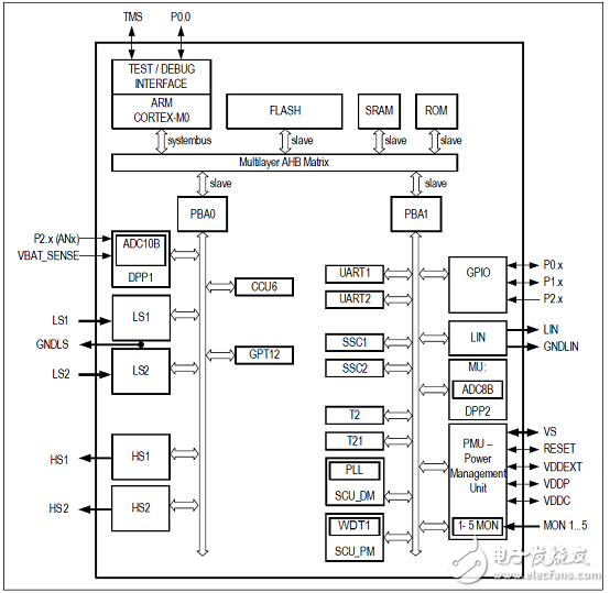
Figure 1. TLE9842-2QX block diagram
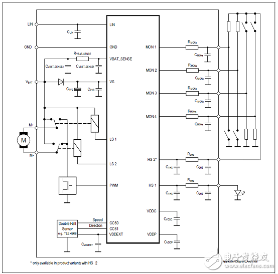
Figure 2. TLE9842-2QX simplified application block diagram
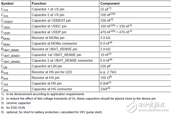
Figure 2 shows the external component table of the application block diagram:
TLE984x Series Evaluation Board
The TLE984x Evaluation Board offers complete evaluation of all functions and peripherals of the TLE984x product family. This board is designed to provide a fast and easy start of evaluation, for Infineons embedded Power TLE984xdevice family. Initialy, the evaluation board brings several interfaces and interconnections.
The TLE984x device is placed in the center of the PCB. A socket provides the possibility to test and evaluate all ICsout of the TLE984x device family. Every pin of the IC is connectable via rows of pinheader. The board is protectedagainst reverse polarity of input voltage In addition to that, a scew-connector is placed near the relay to contact and drive a DCmotor(example: window lift motor).
The evaluation board provides an on board debugger. It provides a SWDDebugconnection and a virtual COM port for serial UART communication. Highside and Lowside switches and VDDEXT are connectable via 4mm standard laboratory wires.
The High-Voltage-Monitor pins can be triggered with dedicated pushbuttons. For analog input values ​​a potentiometer is connected to PIN P2.2. The LIN connection is able to be configured to master and slave mode.
TLE984x series evaluation board target application:
Motor Control & Drives
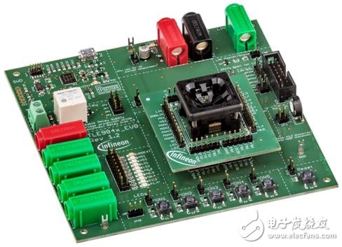
Figure 2. Outline drawing of the TLE984x series evaluation board
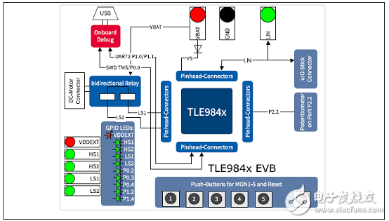
Figure 3. TLE984x Series Evaluation Board Block Diagram
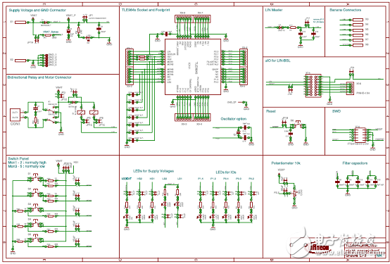
Figure 4. TLE984x Series Evaluation Board Circuit Diagram (1)
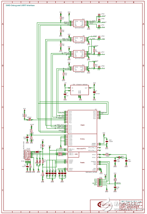
Figure 5. TLE984x Series Evaluation Board Circuit Diagram (2)
TLE984x Series Evaluation Board Bill of Materials (BOM):
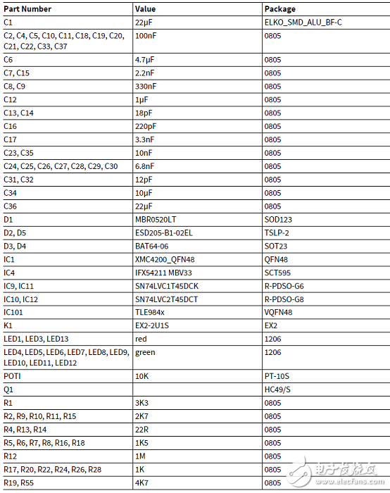
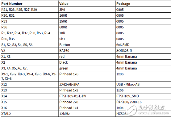
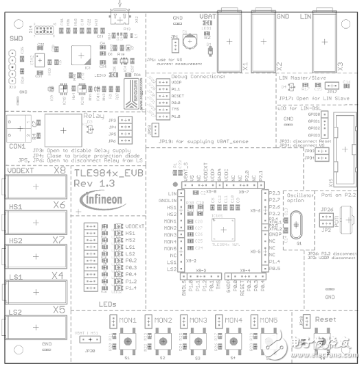
Figure 6. Layout diagram of the TLE984x series evaluation board PCB components
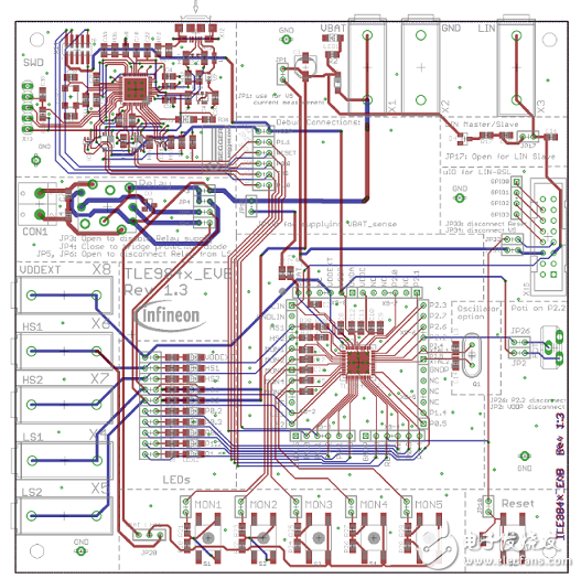
Figure 7. TLE984x series evaluation board PCB design composite diagram
ZGAR MINI
ZGAR electronic cigarette uses high-tech R&D, food grade disposable pod device and high-quality raw material. All package designs are Original IP. Our designer team is from Hong Kong. We have very high requirements for product quality, flavors taste and packaging design. The E-liquid is imported, materials are food grade, and assembly plant is medical-grade dust-free workshops.
From production to packaging, the whole system of tracking, efficient and orderly process, achieving daily efficient output. We pay attention to the details of each process control. The first class dust-free production workshop has passed the GMP food and drug production standard certification, ensuring quality and safety. We choose the products with a traceability system, which can not only effectively track and trace all kinds of data, but also ensure good product quality.
We offer best price, high quality Vape Device, E-Cigarette Vape Pen, Disposable Device Vape,Vape Pen Atomizer, Electronic cigarette to all over the world.
Much Better Vaping Experience!


E-Cigarette Vape Pen,Disposable Device Vape,Vape Pen Atomizer,Latest Disposable E-Cigarette OEM vape pen,OEM electronic cigarette,ZGAR Mini
ZGAR INTERNATIONAL(HK)CO., LIMITED , https://www.zgarecigarette.com