
ADC0809 is a CMOS process 8-channel, 8-bit successive approximation A/D analog-to-digital converter manufactured by National Semiconductor. It has an 8-channel multiplexer inside, which can latch the decoded signal according to the address code and only strobe one of the 8 analog input signals for A/D conversion. At present, it is only common in the application design of single-chip microcomputer.
Interface address of ADC0809 and MCU----ADC0809 pinThe ADC0809 chip is a 28-pin dual in-line package with pinouts as shown below.
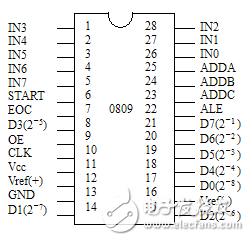
The functions of the main signal pins of ADC0809 are described as follows:
IN7~IN0——analog input channel
ALE - Address Latch Enable Signal. Corresponding to the ALE upper edge, the A, B, and C address states are sent to the address latch.
START - converts the start signal. At the rising edge of START, ADC0809 is reset; when the falling edge is START, the chip is started and A/D conversion is started; during A/D conversion, START should be held low. This signal is sometimes abbreviated as ST.
A, B, C - address line. Channel port select line, A is the low address, C is the high address, and the pin map is ADDA, ADDB and ADDC. The correspondence between the address status and the channel is shown in Table 9-1.
CLK - clock signal. There is no clock circuit inside the ADC0809, and the required clock signal is provided by the outside world, so there is a clock signal pin. Usually use a clock signal with a frequency of 500KHz
EOC - conversion end signal. EOC=0, conversion is in progress; EOC=1, the conversion ends. The status signal can be used as a status flag for the query and can also be used as an interrupt request signal.
D7 ~ D0 - data output line. It is a three-state buffered output form that can be directly connected to the data line of the microcontroller. D0 is the lowest and D7 is the highest
OE - Output enable signal. It is used to control the data obtained by the three-state output latch output to the microcontroller. OE=0, the output data line is high impedance; OE=1, the output converted data.
Vcc - +5V power supply.
Vref - The reference supply reference voltage is used to compare with the input analog signal as a reference for successive approximations. Its typical value is +5V (Vref(+)=+5V, Vref(-)=-5V).
Interface Address of ADC0809 and MCU----Interface Design of A/D Converter ADC0809 and MCS-51 MicrocontrollerThe ADC0808/0809 eight-bit successive approximation A/D converter is a monolithic CMOS device that includes an 8-bit A/D converter, an 8-channel multiplexer, and microprocessor-compatible control logic.
The 8-channel multiplexer can directly connect to any of the eight single-ended analog signals. The ADC0809 pin has a functional resolution of 8 bits. The maximum non-adjustable error ADC0808 is less than ±1/2LSB, and ADC0809 is less than ±1LSB. Single +5V power supply, analog input range is 0~5V. It has a latched three-state output and the output is compatible with TTL. The power consumption is 15mw. It is not necessary to make zero and full scale adjustments.
The conversion speed depends on the chip's clock frequency. Clock frequency range: 10~1280KHZ When CLK=500KHZ, the conversion speed is 128μs.
IN0~IN7: Analog input port of 8 input channels. 2-1~2-8: 8-bit digital output port.
START, ALE: START is the start control input port, and ALE is the address latch control signal port. These two signal terminals can be connected together, and when a positive pulse is input through software, the analog/digital conversion is started immediately.
EOC, OE: EOC is the conversion end signal pulse output port, OE is the output enable control port. These two signals can also be connected together to indicate the end of analog/digital conversion. The level of OE is changed from low to high, and the tristate output lock is turned on. The memory outputs the digital result of the conversion result to the data bus.
REF(+), REF(-), VCC, GND, REF(+) and REF(-) are reference voltage inputs, VCC is the main supply input, and GND is the ground. Typically REF(+) is tied to VCC and REF(-) is tied to GND. CLK: Clock input.
3-bit address strobe coding table for 3, 8 analog switches ADDA, B, C
The three-bit address strobe input of the 8-way analog switch selects the corresponding input channel. Input channel corresponding to the address code CBA0000111100110011010
10101IN0IN1IN2IN3IN4IN5IN6IN7
A membrane switch consists of various layers laminated together. The layers of a basic membrane switch construction include: a membrane overlay, spacer, printer circuit, rear adhesive, and tail filler. Depending on the environment and requirements of the application into which the membrane switch plugs into, the construction can vary.
Membrane Switch Assemblies,Lcd Display Membrane Switch,Tactile Membrane Switch Keypad,Overlay Tactile Membrane Switch
KEDA MEMBRANE TECHNOLOGY CO., LTD , https://www.kedamembrane.com