
The L6563 is a transition mode (TM) current-mode PFC controller from ST.
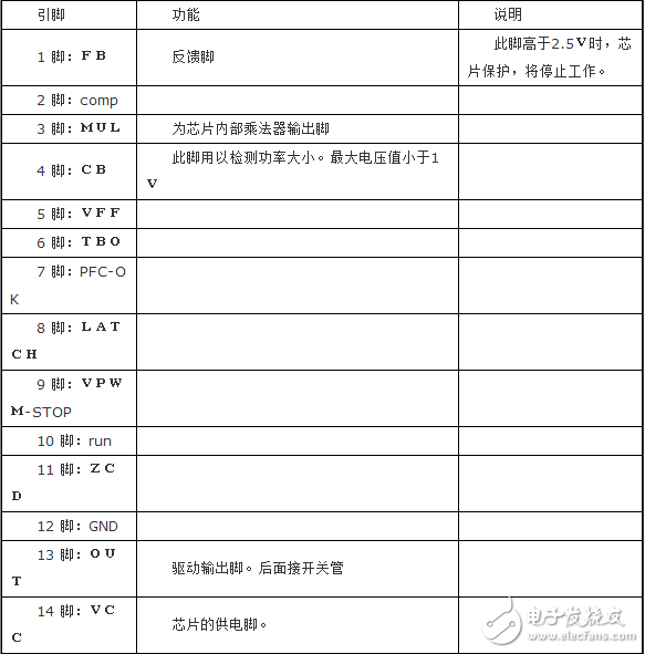
The L6563 contains not only the basic circuitry of a standard TM-PFC controller (such as voltage error amplifiers, multipliers, PWM comparators, zero current detectors, control logic and MOSFET gate drivers, etc.) but also input voltage feedforward (1/V2). Unit circuit such as correction), tracking boost, remote on/off control, DC-DC converter PWM control IC interface and protection circuit, and many improvements and additional functions. Pin Description for L6563
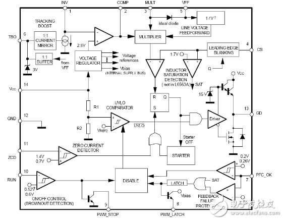
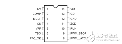
1. INV: Inverting input of the error amplifier. The output voltage information of the PFC pre-regulator flows into this pin through a resistor divider. The normal characteristic of this pin is high impedance, but if the tracking Boost function is used, an internal current generator programmed with TBO (6-pin) will be activated. It will draw current from this pin to change the output voltage, so it tracks the main voltage.
2. COMP: The output of the error amplifier. A compensation network needs to be added between this pin and INV (1 pin) to achieve control loop stability and ensure high PF and low THD.
3. MULT: The main input of the multiplier. This pin is connected to the rectified main voltage terminal by a resistor divider and provides a sinusoidal reference to the current loop. The voltage on this pin is also used to get the rms information of the main voltage.
4. CS: Input to the PWM comparator. The current flowing into the MOSFET is sensed by a resistor, and the sensed voltage is added to this pin to compare with the internal reference to determine the MOSFET switch. A second comparison level of 1.7V to detect abnormal currents (eg, due to BOOST inductive protection), once this happens, turn off the IC and reduce its losses to almost the same level as when starting, PWM_LATCH( 8 feet) is set to high level. This feature is not available in the L6563A.
5. VFF: The second input of the 1/V2 multiplier. A capacitor and shunt resistor must be connected from this pin to GND. They complete the internal peak hold circuit, which obtains information from the rms value of the main voltage. The voltage DC level of this pin is equal to the peak voltage of the MULT pin (pin 3). This voltage compensation depends on the control loop gain of the main voltage. Do not connect this pin directly to GND.
6, TBO: Track BOOST function. This pin provides a buffered VFF voltage. The current flowing from INV (1 pin) is defined by connecting this pin to GND through a resistor. In this case, the output voltage changes in proportion to the main voltage (tracking BOOST). If you do not use this feature, leave this foot unconnected.
7. PFC_OK: PFC pre-regulates the output voltage monitoring or enabling function. This pin senses the PFC pre-regulated output voltage by a resistor divider and is also used for protection purposes. If the voltage of this pin exceeds 2.5V, the IC is turned off, its loss is reduced to near the level at startup and this condition is locked. The PWM_LATCH pin is set high. Only when Vcc is powered back on can it work again. This feature is used to protect the feedback loop from failure. If the voltage of this pin is lower than 0.2V, the IC is turned off and its loss is reduced. This pin voltage must be re-started above the 0.26V IC. If these features are not required, keep the voltage of this pin between 0.26 and 2.5V.
8. PWM_LATCH: Output pin of the fault signal. This pin maintains high impedance characteristics during normal operation. If the PFC_OK (7-pin) voltage is detected to be higher than 2.5V, or the CS (4-pin) voltage is detected to be higher than 1.7V, the voltage of this pin is set high. Normally, this pin is used to stop the DC-DC operation behind it, enabling its PWM controller by calling a latch. If not, leave this foot unconnected.
9. PWM_STOP: Output pin of the fault signal. This pin characteristic is high impedance during normal operation. If the IC is enabled because the RUN (10-pin) voltage is below 0.5V, the pin voltage is pulled low to GND. In general, this pin is used to stop the DC-DC converter operation at its back end by enabling its PWM controller. If not, leave this foot unconnected.
10. RUN: Remote switch control terminal. A voltage below 0.52V turns off (unlocks) the IC and reduces its loss to a very low level. PWM_STOP is asserted low. The IC restarts after the voltage of this pin is higher than 0.6V. Use this function to connect to VFF (5-pin) directly or through a resistor divider to use this function for undervoltage protection (AC main voltage undervoltage). If you do not need to connect this function to INV (1 pin).
11, ZCD: BOOST inductor demagnetization sensing input in the traditional mode. A negative edge triggers the MOSFET turn-on.
12, GND: ground. The IC signal portion and the gate-driven current return terminal.
13, GD: gate drive output. The output of the totem pole drives the power MOSFET and IGBT, driving peak currents up to 600mA output and 800mA sinking. This pin's high level voltage is clamped at 12V to avoid exceeding the gate voltage.
14, VCC: IC signal part and gate drive supply voltage.
Steel Wire Armored Underground Power Cable
Standard: BS 5467 BS 6346 IEC 60502
Rated Voltage: 0.6/1kV
Armour:
Single Core: AWA (Aluminium Wire Armour)
Multi-Core: SWA (Steel Wire Armour)
Certificates: Third party test reports
Applications: Armored Cable for power networks, industrial plants, switch-boards, underground and in cable ducting where better mechanical protection is required.
Swa Cable,Armoured Cable,Steel Armoured Cable,Outdoor Armoured Cable
Shenzhen Bendakang Cables Holding Co., Ltd , https://www.bdkcables.com