Ten years without regrets, stick to the silicon substrate
In 1993, former Jiangxi University and Jiangxi University of Technology merged to form a new Nanchang University. In the autumn of that year, Jiang Fengyi proposed to establish a material preparation laboratory to engage in research work on new types of luminescent materials. Although the construction funds of the school had already been allocated, the school leaders still made a decisive decision and loaned 600,000 yuan to build the laboratory. Since then, the prelude to the research on high-tech products - blue light materials and devices in the red land has been opened. Due to the serious shortage of funds and the inability to buy advanced instruments and instruments, Jiang Fengyi led a group of young people to work hard, researching, designing and assembling the relevant instruments and equipment of their own experiments, constantly summing up and accumulating experience from practical operation and gradually optimizing. Research equipment, mastered a lot of new experimental skills, and then independently carried out research work on blue-emitting materials for international frontier topics.
The replacement of incandescent lamps and fluorescent lamps by semiconductor LED lamps is the trend of the times. In this field, countries such as Japan and the United States have taken the lead, monopolizing the sapphire substrate and silicon carbide substrate semiconductor LED technology routes. Under this circumstance, the Research Center for Luminescent Materials and Devices Engineering of the Ministry of Education (Nanchang University) has creatively developed a new semiconductor LED technology route---the silicon-based semiconductor LED technology route, which has changed the core of monopoly in Japan and the United States. The technical situation has rewritten the history of the world's LED.
After more than 3,000 experiments, Jiang Fengyi and his team withstood the suspicion and incomprehension of the industry, adhered to the silicon substrate technology without regrets, and finally moved from tracking to leaping, inventing a special transition layer and specific The silicon surface processing technology overcomes the huge lattice mismatch and thermal mismatch between the epitaxial layer and the substrate. On the first generation of semiconductor silicon materials, the third generation semiconductor GaN with high quality quantum well structure has been successfully fabricated. Materials, successful development of silicon substrate blue, green and white led. Its technical indicators such as luminous efficiency, reliability and device life are in an international leading position in similar research, and it is the first in the world to realize the mass production of this new technology product.
The cost of the led chip produced by this result is significantly lower than that of the sapphire substrate and the silicon carbide substrate LED chip. This technology is a new technology for rewriting history for blue LEDs. The results also produced the world's first silicon-based LED full-color display (where blue and green LEDs were fabricated on a silicon substrate). The achievement was awarded the first National Semiconductor Lighting Engineering Innovation Competition R&D Innovation Award in July 2006.
Industrialization continues to write the legend of silicon substrate
Under the reality that many scientific research results are unable to find funds and cannot be industrialized, the silicon substrate LED technology route has attracted joint investment of five international venture capital funds. The US$52 million investment has been fully in place, and a high-tech enterprise specializing in the production of GaN-based LED epitaxial materials and chips on silicon substrates, Jingneng Optoelectronics (Jiangxi) Co., Ltd., has been established in Nanchang, Jiangxi. Crystal Energy Optoelectronics has also become another development platform for the industrialization of silicon substrates. At the same time, Jingneng Optoelectronics has continued to write the Chinese legend of silicon substrate epitaxial chips.
From school to business, from laboratory technology to industrial production, from researchers to business managers, the group successfully completed the transformation of roles. One of the foundations for a smooth transition is that the team is a collective of "can be literate, red and specialized." Here, the text, the Wu and the Red, were given a new connotation by them. Text: It has a solid theoretical knowledge; Wu: is a skilled hands-on test ability; special: refers to the "literary and civil" function; red: is a person's ideological and moral quality.
The second foundation for a smooth transition is the model of "corporateization of scientific research work" that the collective has long adhered to. In the laboratory research stage, they established a pilot production line, which combines basic research, application development research, and pilot test, and firmly targets the research in "industrialization"; the business model of the enterprise is moved to the laboratory. In addition to the R&D team, many skilled workers were recruited and three shifts were carried out to conduct experimental research. "The researcher does the experiment during the day and delivers it to the technical workers in the evening according to the pre-programmed procedures. The next morning, the work results have already come out." This process, in this "laboratory enterprise", is repeated every day. It has won valuable time for research and development and accumulated valuable experience for industrialization.
The team devoted all its efforts to the process of industrialization. In less than a year, it built a modern enterprise with international standards in a desolate land, and realized it in less than half a year. It has the original innovative results---the mass production of silicon substrate LED materials and chips, with an annual production capacity of 3 billion silicon substrate LED chips (low power). At present, the company is developing LED chips for color TV backlights and LED chips for street lamps. The medium and long-term development goal is to be a leading manufacturer of high-end LED chips with international characteristics. The next step in research and development is to develop cost-effective LED chips (high power) for semiconductor lighting to enter thousands of households as soon as possible.
Jiang Fengyi and his team have obtained and published more than 50 invention patents in this field, which has laid an important foundation for the development of China's LED industry in terms of technical property rights. The research results of the collective research and development "silicon substrate GaN-based LED epitaxial materials and chips "The first internationally successful industrialization is the epitome of China's semiconductor LED industry from "Made in China" to "Created in China."

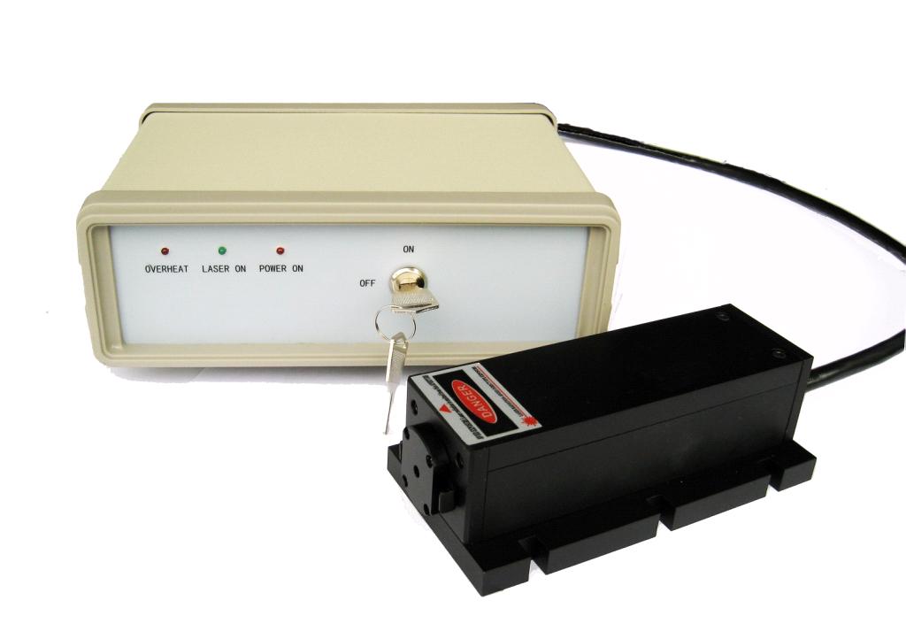
Coupletech Co., Ltd. Supply CW Laser models for medical instruments and scientific research, consists of UV laser GN-355, Low noise blue laser GL-473, Low noise green laser DL-532nm, Signal mode green laser CS-532, Sodium Yellow Laser GL-556, Light yellow laser GL-561, Orange yellow laser GL-593 and Infrared laser GL-1064, and these laser models cover a wide range of wavelengths: 355nm, 473nm, 532nm, 556nm, 561nm, 593nm, 1064nm, and son. The application of CW laser models is for Fluorescence stimulated for biological medical instruments, Interferometry, laser hologragh, flow cytometry, physical instruments, scientific research and so on. The average output power is 10 mW ~ 2000 mW, beam diameter at the aperture is ~ 1.5mm. Besides, single mode fiber coupled or customized is optional.


Diode Pumped CW,Diode Pumped Solid State Laser,Solid State Laser Diode
Coupletech Co., Ltd. , http://www.coupletech.com
