
Pick   To:       The design scheme of the two-bus communication module is given, and the relevant circuits involved in the design of the power line interface of the communication module and the two-bus interface circuit are mainly introduced.
introduction
Smart homes require household appliances to be interconnected and interoperable via a network ( bus ) . The bus protocol is the essence of the system. At present, the internationally dominant home network standards are: X10 in the United States , Consumer Bus (CEBus) , Home Bus in Japan (HOME BUS) , and Installation Bus in Europe (EIB) .
The consumer bus uses five types of media: power line, wireless, infrared, twisted pair, and coaxial cable, of which the power line is the most widely used. However, the current characteristics of China's power grid, grid structure, residential distribution and other factors make it difficult for power line carrier communication to achieve the expected communication effect. In order to reduce the interference between power carrier signals, the network system should minimize the introduction of power carrier signals. In the entire network system, the power carrier communication module is used to realize the data exchange between the household appliances and the data collector.
The block diagram of the power carrier communication module is shown in Figure 1 . In the design, AT89S52 is used as the microcontroller, and the power line carrier modem uses the special chip ST7536 . Between AT89S52 and ST7536 , a universal serial communication interface is used, and I2C bus is used to communicate with serial EEPROM . EEPROM uses ferroelectric 24C02. This chip has an unlimited number of erasable functions. The communication of the entire network is realized through the power carrier, and the communication between the module and other devices is realized through the two buses. In this way, the communication module can communicate and control multiple actual devices through software and communication protocols. All data frames use CRC check. AT89S52 and ST7536 are made on external hardware reset, while using AT89S52 internal watchdog function, AT89S52 necessary and ST7536 reset to prevent system crashes caused by network traffic interruption. The multi-way selector switch adopts CD4052 , through which the power carrier and the two buses are selected to realize the time-sharing control of the power carrier communication and the two buses.
Â

Picture 1 Â Block diagram of general communication module

Picture 2 Â Power line interface diagram

Picture 3 Â Power line interface circuit

Picture 4 Â Two bus communication circuit
Picture 5 Â Receive and Carrier Transmit Waveform
Circuit design of power line interface of communication module
Foreign countries have conducted research on power line carrier communication technology very early. Many companies have launched their own power line carrier modem chips and formulated standards for the power line carrier frequency range. There are standards for the North American power grid frequency range (480Y / 277V, 208Y / 120Vac ) of 100KHz-450KHz frequency range and standard for the European regional power grid (400Y / 230Vac) of 9KHz-150KHz. In the standard frequency range, various companies have designed their own power line carrier modem chips based on the characteristics of the local power grid and using various specific proprietary technologies . Because the foreign power line carrier modem chip is designed for the characteristics of the local power grid and the structure of the power grid, and is generally designed for home automation, it is difficult to use it in China. At present, there are one or two power line carrier modem chips that can be barely used in certain application fields. This system uses ST7536 as a modem for power carrier communication.
ST7536 is a modem chip designed by STMicroelectronics for power line carrier communication . In addition to the signal modulation and demodulation function of a general modem chip, it also adds many special signal processing methods for power line applications. At present, it is widely used in the domestic power line carrier communication field, but the application level of each company is different. ST7536 modulation and demodulation technology is a relatively backward FSK method, and its highest baud rate can only reach 1200 bps . In addition, it has no CSMA ( Network Carrier Sense ) function, which limits its application. At present, according to the actual situation of the domestic power grid, ST7536 is a more suitable modem chip in the field of power line carrier communication .
The signal amplitude output from ST7536 is small, the driving ability is weak and there are various harmonics, so it must be amplified and filtered before the signal can be modulated onto the power line through the coupling circuit. The coupling circuit isolates the high voltage from the low voltage to prevent the high voltage from breaking down the communication circuit. Similarly, the carrier signal from the power line must be received by the ST7536 , and the interference signal on the power line is very uncertain and very complex, so a band-pass filter is required to pass the signal between 67.2kHz ~ 87.5kHz ( this system uses 72kHz Carrier frequency ) , and then sent to the receiving end of ST7536 after pre-amplification . The block diagram of the circuit is shown in Figure 2 .
Comprises a block diagram of a left end of ST7536 from ATO and RAI and RX / TX, RX / TX is a digital signal, the conversion control the transceiver. ATO is the transmission output of ST7536 , which is connected to the transmission input of the power line interface. The analog transmission output is adjusted by the automatic level control input circuit. The peak -to- peak value of the maximum output voltage is 6.5V . RAI is the receiving analog input of ST7536 . It is connected to the receiving output of the power line interface. The rms value of the maximum input voltage is 2V . The rms value of the receiving sensitivity is 2mV on channel 1 and channel 2 (600 baud) ; 3mV on channel 3 and channel 4 (1200 baud) . This system uses the latter.
Power line transmitting and receiving circuit
The power line interface circuit is shown in Figure 3 .
Digital signal RX / TX switch state control transistor, provides DC power to the transmission circuit, when the RX / TX is high, the circuit is in the off state, when the RX / TX is low, the circuit is in the ON state, the ATO ST7536 After the signal is amplified by filtering, it is coupled to the power line. In this way, only when the circuit is in carrier wave transmission, the power consumption of the system reaches the maximum value.
In the transmission mode, the power line interface amplifies and filters the transmission signal from the ST7536 chip ATO . The function of the buffer is to protect the ST7536 and drive the next component in the power line interface. The purpose of the low-pass filter (LPF) is to suppress harmonics. The filtered signal is sent to a power amplifier, which drives a power line with an impedance of 1 to 100 Ω through a converter . In addition, the amplifier also performs band filtering to suppress the second harmonic of the transmitted signal.
In the receiving mode, the converter takes the signal from the power line, amplifies it in the pre-amplifier, and sends it to the receiving input RAI of ST7536 . In this mode, make RX / TX high.
Through this circuit , the effective communication distance of 1200m ~ 1500m can be achieved on the power line . If the software design of this system is reused to realize the relay function, the actual communication distance of the power line will be strengthened.
Coupling circuit and its protective measures
In Figure 3 , RY1 is a varistor, which can short-circuit the spikes to prevent damage to the circuit from high voltage, and the coupling transformer TR1 achieves isolation between high voltage and low voltage. Because the frequency of the carrier wave is relatively high, which is much greater than the frequency of the power grid, this makes the carrier signal unimpeded and can isolate high voltage. Capacitor C37 blocks low frequency and high voltage to prevent transformer saturation; the value of resistor R37 is relatively large, and its role is to discharge the capacitor when offline, to prevent high voltage from appearing at both ends of the device plug. D13 is a bidirectional voltage stabilizing diode, that is, a transient suppression diode, which can effectively avoid the breakdown of the circuit behind by high voltage. In addition to the high-voltage pulses on the power line, when the device is just connected to the power supply, about 300 volts of high voltage may be directly applied to the coupling transformer, causing a large current, which can reach tens of amps to hundreds of amps. It is impossible for the voltage regulator to eliminate such pulses. Because the corresponding time of the varistor is slow, it can't meet the requirements of the circuit at all, but the bidirectional voltage regulator can meet the requirements.
Design of two bus interface circuits
The two bus interface circuits are shown in Figure 4 .
This system can realize the control and information acquisition of multiple devices through this circuit. Its loading capacity is determined by another set of bus transmission and reception circuits, and its effective transmission distance is about 1000m . Because it has only two communication lines, it is very simple and convenient to connect the system.
It can be seen from Figure 4 : When TCON and RCON are both low, the bus neither receives nor transmits.
When TCON is high, no matter what level RCON is, the bus is in the transmitting state, because at this time U7-11 is always locked to high level, U7-10 is low, T2 and T4 are cut off, and reception is prohibited; and U6-6 is low, D5 and D6 are off, and TXD2 is transferred to the bus. When TXD2 is high, T1 and T6 are turned on, T3 is turned off, and the voltage on the bus is 12 volts; when TXD2 is low, T1 and T6 are turned off, T3 is turned on, and the voltage on the bus is 0 volts.
When TCON is low and RCON is high, the bus is in the receiving state. At this time, T1 , T3 , and T6 are off, and transmission is prohibited; while T2 and T4 are on, together with T5 , the digital signal on the bus can be passed to RXD2 . The signal transmitted on the bus is a series of digital signals. The high level of this signal is 5V, and the low level is 0V .
Experimental results
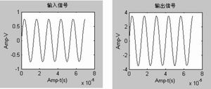
By controlling the RX / TX control pin of ST7536 , the carrier circuit is in the receiving state, add a 72KHz , 0.3V sinusoidal signal between the live line and the neutral line , observe the waveform of the ST7536 24 pin with an oscilloscope , the normal should be 72KHz , 1.5 ± 0.5V , frequency offset adjustment C35-C37 , each increase of 1nF , the center frequency decreases by 2.4KHz . The carrier receiving signal is shown in Figure 5 ; when the initial carrier circuit is in the transmitting state, connect the 10th pin of the ST7536 , that is, the test pin, to VCC, connect a 5.1 Ω power resistor between the neutral and live wires, and observe with an oscilloscope The waveform between the neutral line and the live line should normally be 72KHz , and the peak-to-peak value should be greater than or equal to 7V . If the signal distortion is adjusted, adjust the relative capacitance. The carrier signal is shown in Figure 5 .
Conclusion
The design of this communication module adopts the combination of power line carrier and two bus communications. In a power line subnet, the use of power line communication is reduced as much as possible, so that the interference signal in the same frequency band caused by the power carrier signal in the power line is well improved. Use two bus communication to achieve communication between the communication module and the bottom layer. In order to realize the network interconnection and interoperability of household appliances and building automatic control systems, it has been practically applied in the field of building automatic control and multi-meter collection system
Fiber Optic Accessories,Fiber Optic Cable Connectors,Fiber Optic Adapter,Fiber Cable Connectors
Huizhou Fibercan Industrial Co.Ltd , https://www.fibercan-network.com