
introduction
LEDs have contributed to the process of urbanization, and all kinds of nightscape lights and advertising displays are increasingly filling people's novel eyes. In the past, neon illuminators only had two states: light and extinction. The brightness was suddenly changed, which often gave people a feeling of pattern change. Now many neon lights have realized the gradual change of the brightness of the illuminator. The neon pattern is softer and smoother. The change of brightness of the control illuminator can be divided into analog method and digital method. The method of controlling the brightness of the illuminant by controlling the D/A converter by the single-chip microcomputer has the characteristics of simple circuit, convenient maintenance and adjustment, and is the development direction of the current neon control. . Neon illuminants are mainly gas discharge lamps. Now with the development of high-brightness LEDs, LED lamps with long life and low energy consumption are becoming more and more widely used. Here we discuss how to control the brightness variation of multiple LEDs under the control of the microcontroller using the DAC0832.
1 hardware circuit design
The brightness of the three LEDs is gradually changed in sequence by the single chip microcomputer and the D/A conversion chip DAC0832, thereby realizing the effect of the rotation of the lamp. The following three main issues are considered in the design:
(1) Interface circuit design of DAC0832 and single chip microcomputer.
(2) Design of the reference voltage source.
(3) Circuit design that simultaneously controls the brightness of multiple LEDs to change brightness according to different rules.
1.1 DAC0832 and microcontroller interface circuit
The ADC0832 is enabled to implement analog-to-digital conversion in either single buffer or double buffer. The multi-buffer mode is used when multiple ADC0832 are matched. In this design, only one ADC0832 can be used for work. Therefore, the single buffer mode is used to input data to its 8-bit data input port, and then a write trigger pin WR1 is sent. With a low level pulse, the chip converts the received digital quantity into an analog output. The output is a current input signal, and the brightness of the control LED needs to be realized by voltage. Therefore, an external current-voltage conversion circuit composed of an operational amplifier is required, and the interface circuit of the ADC0832 and the single-chip microcomputer is as shown in FIG. 1:

In the figure, since the chip select terminal CS is connected to P217, when starting the DAC0832 to start conversion, the P217 pin of the microcontroller needs to be set low.
The output current is converted into a voltage by an operational amplifier. If the digital quantity to be converted is B, the corresponding output voltage value is:
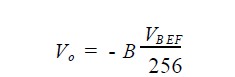
Where VREF is the external reference voltage, the output voltage is up to 0 V, and the lowest is -VREF. If the reference voltage is 5 V, the minimum output voltage is -5 V. To meet the requirements of the negative voltage output, the op amp's power supply voltage is VCC. To be higher than 5 V, VEE is lower than -5 V. In this design, the operational amplifier uses LM324 chip, the power supply voltage VCC is 10 V, and the VEE is -10 V.
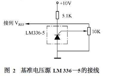
1.2 Design of the reference voltage
To ensure the accuracy and accuracy of the DAC0832 digital-to-analog conversion, a highly stable reference voltage must be provided. In the digital-to-analog converter, a bandgap reference voltage source or a buried Zener voltage regulator tube is generally selected.
The design uses the LM336-5 buried Zener diode, which has the characteristics of low price and convenient use. The wiring is shown in Figure 2:
1.3 How to control the brightness of multiple LEDs at the same time
In the design, three LEDs need to be controlled. The brightness and variation of each LED are different. The ADC0832 has only one analog output. In order to control the brightness of the three LEDs, a multi-channel electronic switch is needed. In this example, The CD4051 is selected. The pin diagram of the chip is as follows:

The chip is a commonly used 8-way to 1-way multi-channel electronic switch with a working voltage of up to 32 V. Which channel is strobed by the ABC three address pins.
Because the previously converted voltage has a negative value of -5 V, the operating voltage of CD4051 is VDD = 10 V, VEE = - 10 V, and the address control terminals A, B, and C are decomposed into P210, P211, and P212 of the microcontroller. The port is used to strobe a certain channel. The analog quantity after D/A conversion is connected to the voltage input terminal 3 of the multiplexer, and the output pins 13, 14, 15 respectively control the LEDs D1, D2 and D3.
The DAC0832 only has one analog output. It must use the time-sharing control method to cyclically control the brightness of the three LEDs. When one LED is connected, the other LEDs must keep the original brightness and cannot be extinguished. In order to achieve this, the operation is used here. The amplifier is connected to the form of a voltage follower to control the brightness of the LED, that is, a voltage follower is connected between each output of the multi-channel electronic switch and the LED, and a holding capacitor is connected to the forward input of the operational amplifier to make the input The voltage can be maintained for a period of time and its wiring is as follows:
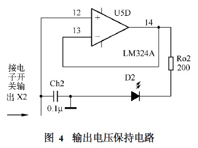
Since the input impedance of the op amp is large, the voltage on Ch2 can be maintained for a period of time, and the output voltage of the op amp can remain constant while the output voltage of the digital-to-analog converter controls other LEDs.
The hardware schematic of the device is shown in Figure 5.

2 software design
The software mainly performs two functions. First, the cycle of each LED is completed. Second, the brightness of each LED is controlled by a program. In this example, the effect of the light rotation is realized, so each LED changes according to the brightness of the triangular wave type, and gradually becomes brighter. When it reaches the brightest time, it is gradually darkened by the brightest, and so on; the brightness of the three LEDs changes. There is a time difference. If an LED goes from dark to light to dark as a period, then D2 lags 1/3 cycle from D1, and D3 lags 1/3 cycle from D2.
2.1 main program design
The LEDs are cycled through the main program loop, and three data representing the brightness of the three LEDs are placed in three consecutive RAM units 30H, 31H, 32H, and the data of the three units is cyclically read in the main program. To DAC0832 conversion, according to the different values ​​in 30H, 31H, 32H, the analog voltage of the conversion output is also different. The MCU controls the multi-channel electronic switch to send different analog voltages to different LEDs, so that each LED has different brightness. In this example, the P2 port is used to control the strobe of the ADC0832 and the strobe of the electronic switch. According to the schematic wiring, the P2 port data corresponding to the LEDs D0, D1, and D2 are 00H, 01H, and 02H, respectively.
2.2 Interrupt program design
The control LED brightness change is realized by the timer T0 timer interrupt program. The T0 interrupt changes the values ​​of 30H, 31H and 32H to change the LED brightness. If the effect of the light rotation is realized, the brightness of the three LEDs should be changed according to the curve of Fig. 6.
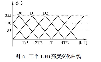
In the figure, the abscissa indicates the time. In one cycle, the brightness of the LED will change according to the triangle law. Let each change period be T, and the change of the second LED D1 lags the first LED D1 by one-third period. Similarly D2 lags D1 by one-third of the cycle.
The abscissa in Fig. 6 represents the brightness, that is, the corresponding numerical value to be converted into an analog quantity. In the main program, the values ​​of the three bytes 30H, 31H, and 32H correspond to the brightness of the three LEDs, and the values ​​of the three bytes 33H, 34H, and 35H are set to control whether the brightness of the three diodes increases or decreases (1 enhancement, 0 attenuation) ). Suppose that D1 corresponds to a brightness of 0 at the beginning, and D0 and D2 correspond to a brightness of 170. The brightness of the three diodes should be increased by D0 and D2, and the brightness of D2 is weakened. The values ​​of the three brightness control bytes are respectively 33H. In 35H, it is 1, and 35H is 0.
With the T0 interrupt to achieve the change of the brightness of the three LEDs, each time the timer interrupt will complete the following functions:
1) The values ​​of 30H, 31H, and 32H are incremented or decremented by 1 according to the values ​​of the three bytes 33H, 34H, and 35H, respectively.
2) When the value of the brightness byte is increased to 255, the corresponding control byte value is cleared. When the brightness byte value is reduced to 0, the corresponding control byte value is set to 1.
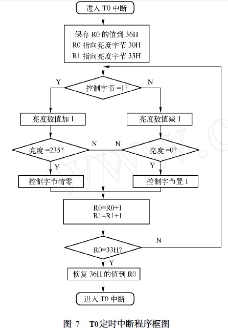
Since the working register R0 is used in the main program and the interrupt subroutine, there is a process of saving and restoring the value in R0 at the beginning and end of the interrupt program.
The block diagram of the interrupt program is:
That is: TH0 = F0H, TL0 = BEH3
3 Conclusion
In this paper, a system based on DAC0832 for LED control is designed. Under the control of single-chip microcomputer, the change of brightness of multiple LEDs is realized by multi-way switch and voltage hold circuit, and the effect of LED light rotation is realized. If you extend this circuit and connect more analog-to-digital converters and multiplexers, you can implement a variety of complex pattern changes. The method of using a voltage holding circuit can also be applied to analog control in other fields.
references:
[1]. DAC0832 datasheet http://
[2]. ADC0832 datasheet http://
[3]. LM324 datasheet http://
[4]. LM336 datasheet http://
[5]. ABC datasheet http://
[6]. CD4051 datasheet http://+_1865305.html.
[7]. P212 datasheet http://+_1557737.html.
[8]. D1 datasheet http://+_2060593.html.
Electric Switch Panel,Marine Switch Panel,Boat Switch Panel Marine ,Automotive Switch Panel
Dongguan Andu Electronic Co., Ltd. , https://www.autoido.com