
1. Case background
2. Brief analysis method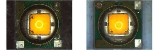
Figure 1. LED appearance photos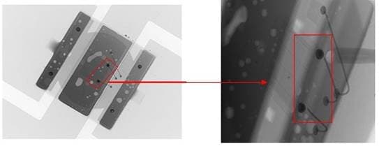
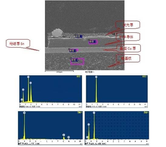
Figure 3. SEM / EDS picture of NG sample profile (150X)
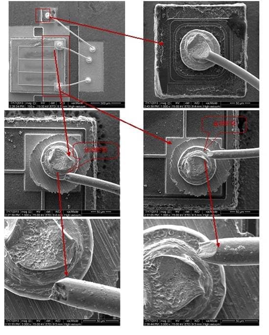
Figure 4. SEM photos of NG samples after unsealing (150X, 1000X, 3000X)
4 Conclusion
Note: Because there are too many actual reports, this article has simplified the content. If there are any shortcomings, one-sidedness, please correct me.
customized stainless steel acoustic structure, high quality grahene hoop system and obvious environmental noise attenuation will open up a pleasant journmey journey for you to enjoy the sound.
Built-in microphone/ Effective noise reduction/ Clear call/ Easy to carry
The LED does not turn on when powered on, and can light up normally when lightly pressed by hand.
2. Brief analysis method
1) X-ray fluoroscopy can clearly find that the two bonding wires on the NG sample connected to the large chip inside the LED have obvious breakage at the end of the bonding point, and the internal end connected to the negative electrode is well bonded. The OK sample did not show any abnormalities.
2) Use chemical methods to corrode the LED surface encapsulation colloid. Observe the internal structure by electron microscope. It can be clearly seen that the two gold wires connected to the positive electrode inside the chip have obvious mechanical stress fracture at the end, and the fracture has necking and metal Mechanical sharpening. The fracture positions are all in the binding neck position, and the binding point is well bound. Cross-sectional observation showed no obvious cracks or air holes and other packaging defects in the LED hemispherical encapsulant.
3) From the internal structure of the LED after unsealing, this sample is different from the common LED package. The positive bonding point on the chip is the second bonding point with tail (generally the second bonding point is the weak strength of the chip package Point, easy to break and other abnormalities), and the binding point on the negative electrode of the frame is the first binding point of the ball shape. It is the position of the second binding point with tail that mechanically breaks, which is higher than the first binding point of the negative pole in three-dimensional space, and is more susceptible to external mechanical stress.
Figure 1. LED appearance photos
Figure 2. X-ray perspective photo of NG sample
Figure 3. SEM / EDS picture of NG sample profile (150X)
Figure 4. SEM photos of NG samples after unsealing (150X, 1000X, 3000X)
3. Failure mode analysis
LED failure modes mainly include: chip failure, package failure, thermal stress failure, mechanical stress failure, electrical overstress failure and bonding failure. The NG samples were all failures caused by mechanical stress.
1) Wafer failure: Wafer failure refers to the failure of the wafer itself or other causes of wafer failure. There are many reasons for this failure: wafer cracks are due to inappropriate bonding process conditions, resulting in greater stress, and the thermomechanical stress generated with heat accumulation is also strengthened, resulting in micro cracks in the wafer. The current injected at this time will further aggravate the micro-crack and make it expand continuously until it completely fails. Secondly, if there is damage to the active area of ​​the chip, it will gradually degrade until it fails during power-on, and it will also cause the luminescence of the lamp to be severe until it is not bright during use. Furthermore, if the wafer bonding process is not good, the wafer bonding layer will be completely detached from the bonding surface during use, which will cause open failure of the sample, and it will also cause the "dead lamp" phenomenon of the LED during use. The cause of the poor wafer bonding process may be due to the expiration of the used silver paste (insulating adhesive) or too long exposure time, the amount of silver paste (insulating adhesive) used is too small, the curing time is too long, the solid crystal base surface is contaminated, etc. .
2) Package failure: Package failure refers to device failure due to improper package design or production process. The epoxy resin material used for encapsulation will cause degradation during use, which will reduce the life of the LED. Such degradation problems include: light transmittance, refractive index, expansion coefficient, hardness, water permeability, air permeability, filler performance, etc., among which light transmittance is the most important. For packaging, another important factor that affects LED life is corrosion. In the use of LEDs, the main cause of corrosion is that water vapor has penetrated into the packaging material, resulting in the deterioration of the leads and the corrosion of the PCB copper wires. Sometimes, the movable conductive ions introduced with the water vapor will reside on the surface of the chip, resulting in leakage. In addition, a device with poor packaging quality will have a large number of residual bubbles inside the package, and these residual bubbles will also cause corrosion of the device.
3) Thermal overstress failure: The increase in the junction temperature of the high-power LED will cause the epoxy resin material to change, thereby increasing the thermal resistance of the system, causing the heated surface between the chip and the package to degrade, and eventually causing the package to fail.
4) Electrical overstress: If the LED is subjected to overcurrent (EOS) or electrostatic shock (ESD), it will cause the chip to open circuit, resulting in electrical overstress failure. For example, GaN is a wide bandgap material with high resistivity. If this type of wafer is used, the induced charge generated by static electricity during the production process is not easy to disappear. When it accumulates to a considerable degree, a high electrostatic voltage can be generated. This voltage will occur once the voltage exceeds the capacity of the material The breakdown phenomenon and discharge make the device ineffective.
5) Bonding failure: Inadequate bonding conditions in the LED manufacturing process. If the bonding force is too large, the wafer will be crushed, otherwise the bonding strength of the device will be insufficient, making the device easy to loose, or no good bonding is formed at all. interface.
6) Mechanical stress failure: During the LED SMT process flow, testing or transportation, external fixtures, molds or other hard materials hit the LED lamp package, causing the internal structure to momentarily shift and break the internal binding line. This type of failure is more likely to be found in softer packages.
4 Conclusion
The cause of failure of the LED of the failed sample is that it does not light up, and the light pressure of the hand can normally emit light (open circuit): the NG sample is affected by external mechanical stress and the mechanical bonding of the second binding point on the internal wafer occurs.
Note: Because there are too many actual reports, this article has simplified the content. If there are any shortcomings, one-sidedness, please correct me.
Sports can't be abandoned more freely
Close ergonomic design, close to the ear, even wearing for a long time can also enjoy comfortable experience.
And can form a triangular stable support with the ear, even if running and riding, vigorous fitness is still close to the ears, wildly shake off.
Professional sound engineering technology
Case Cube/acoustic clear sound reproductioncustomized stainless steel acoustic structure, high quality grahene hoop system and obvious environmental noise attenuation will open up a pleasant journmey journey for you to enjoy the sound.
Built-in microphone/ Effective noise reduction/ Clear call/ Easy to carry
Bluetooth In Ear Headset,Wireless In Ear Headset,In Ear Headset Wireless,Headset Wireless In Ear
Guangzhou HangDeng Tech Co. Ltd , https://www.hangdengtech.com